
User Manual


Apollo3 Blue Datasheet
DS-A3-0p9p1 Page 50 of 909 2019 Ambiq Micro, Inc.
All rights reserved.
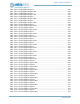
G3 G6 - - RSTN External Reset Input
Input/
Output
RF
J2 H8 - - RFIOM RF I/O Negative Analog
J1 H9 - - RFIOP RF I/O Positive Analog
J3 - - - TXEN Transmitter Enable Output
GPIO
H4 F6 0
0SLSCL
I
2
C Slave Clock
Input
1 SLSCK SPI Slave Clock Input
2 CLKOUT Programmable Output Clock Output
3 GPIO00 General Purpose I/O
Input/
Output
4RSVReserved
5MSPI4
MSPI Master Interface Signal 4
See “MSPI Connection” on page 393.
Input/
Output
6RSVReserved
7 NCE0
IO Master N Chip Select 0
Table 564, “NCE Encoding Table,” on page 382
Output
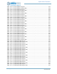
G4 G5 1
0 SLSDAWIR3
I
2
C Slave I/O Data
SPI Master 3 3 Wire Data
Bidirec-
tional
Open
Drain
1 SLMOSI SPI Slave Input Data Input
2 UART0TX UART0 Transmit Output
3 GPIO01 General Purpose I/O
Input/
Output
4 RSV Reserved Input
5MSPI5
MSPI Master Interface Signal 5
See “MSPI Connection” on page 396.
Input/
Output
6RSVReserved
7 NCE1
IO Master N Chip Select 1
Table 564, “NCE Encoding Table,” on page 382
Output
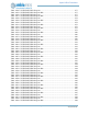
F4 G4 2
0 UART1RX UART1 Receive Input
1 SLMISO SPI Slave Output Data Output
2 UART0RX UART0 Receive Input
3 GPIO02 General Purpose I/O
Input/
Output
4RSVReserved
5MSPI6
MSPI Master Interface Signal 6
See “MSPI Connection” on page 393.
Input/
Output
6RSVReserved
7 NCE2
IO Master N Chip Select 2
Table 564, “NCE Encoding Table,” on page 382
Output
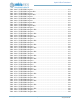
Table 1: Pin List and Function Table
BGA
Pin
Number
CSP Pin
Number
GPIO Pad
Number
Function
Select
Number
Pad Function
Name
Description Pin Type