
User Manual


Apollo3 Blue Datasheet
DS-A3-0p9p1 Page 489 of 909 2019 Ambiq Micro, Inc.
All rights reserved.
11.7.2.44GPIOOBS Register
GPIO Observation Mode Sample register
OFFSET: 0x000000DC
INSTANCE 0 ADDRESS: 0x400100DC
GPIO Observation mode sample register
11.7.2.45ALTPADCFGA Register
Alternate Pad Configuration reg0 (Pads 3,2,1,0)
OFFSET: 0x000000E0
INSTANCE 0 ADDRESS: 0x400100E0
This register has additional configuration control for pads 3, 2, 1, 0
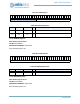
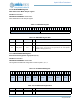
Table 711: GPIOOBS Register
3
1
3
0
2
9
2
8
2
7
2
6
2
5
2
4
2
3
2
2
2
1
2
0
1
9
1
8
1
7
1
6
1
5
1
4
1
3
1
2
1
1
1
0
0
9
0
8
0
7
0
6
0
5
0
4
0
3
0
2
0
1
0
0
RSVD OBS_DATA
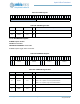
Table 712: GPIOOBS Register Bits
Bit Name Reset RW Description
31:16 RSVD 0x0 RO
RESERVED
15:0 OBS_DATA 0x0 RW
Sample of the data output on the GPIO observation port. May have async
sampling issues, as the data is not synronized to the read operation.
Intended for debug purposes only
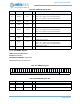
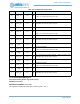
Table 713: ALTPADCFGA Register
3
1
3
0
2
9
2
8
2
7
2
6
2
5
2
4
2
3
2
2
2
1
2
0
1
9
1
8
1
7
1
6
1
5
1
4
1
3
1
2
1
1
1
0
0
9
0
8
0
7
0
6
0
5
0
4
0
3
0
2
0
1
0
0
RSVD
PAD3_SR
RSVD
PAD3_DS1
RSVD
PAD2_SR
RSVD
PAD2_DS1
RSVD
PAD1_SR
RSVD
PAD1_DS1
RSVD
PAD0_SR
RSVD
PAD0_DS1
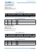
Table 714: ALTPADCFGA Register Bits
Bit Name Reset RW Description
31:29 RSVD 0x0 RO
RESERVED