
User Manual


Apollo3 Blue Datasheet
DS-A3-0p9p1 Page 475 of 909 2019 Ambiq Micro, Inc.
All rights reserved.
11.7.2.20CFGG Register
GPIO Configuration Register G (Pads 48-49)
OFFSET: 0x00000058
INSTANCE 0 ADDRESS: 0x40010058
GPIO configuration controls for GPIO[49:48]. Writes to this register must be unlocked by the PADKEY
register.
3 GPIO40INTD 0x0 RW
GPIO40 interrupt direction.
INTDIS = 0x0 - INCFG = 1 - No interrupt on GPIO transition
INTBOTH = 0x1 - INCFG = 1 - Interrupt on either low to high or high to low
GPIO transition
INTLH = 0x0 - INCFG = 0 - Interrupt on low to high GPIO transition
INTHL = 0x1 - INCFG = 0 - Interrupt on high to low GPIO transition
2:1
GPIO40OUT-
CFG
0x0 RW
GPIO40 output configuration.
DIS = 0x0 - FNCSEL = 0x3 - Output disabled
PUSHPULL = 0x1 - FNCSEL = 0x3 - Output is push-pull
OD = 0x2 - FNCSEL = 0x3 - Output is open drain
TS = 0x3 - FNCSEL = 0x3 - Output is tri-state
0 GPIO40INCFG 0x0 RW
GPIO40 input enable.
READ = 0x0 - Read the GPIO pin data
RDZERO = 0x1 - INTD = 0 - Readback will always be zero
READEN = 0x1 - INTD = 1 - Read the GPIO pin data
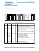
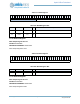
Table 663: CFGG Register
3
1
3
0
2
9
2
8
2
7
2
6
2
5
2
4
2
3
2
2
2
1
2
0
1
9
1
8
1
7
1
6
1
5
1
4
1
3
1
2
1
1
1
0
0
9
0
8
0
7
0
6
0
5
0
4
0
3
0
2
0
1
0
0
RSVD
GPIO49INTD
GPIO49OUTCFG
GPIO49INCFG
GPIO48INTD
GPIO48OUTCFG
GPIO48INCFG
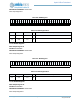
Table 664: CFGG Register Bits
Bit Name Reset RW Description
31:8 RSVD 0x0 RO
RESERVED
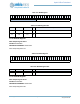
Table 662: CFGF Register Bits
Bit Name Reset RW Description