
User Manual

Apollo3 Blue Datasheet
DS-A3-0p9p1 Page 448 of 909 2019 Ambiq Micro, Inc.
All rights reserved.
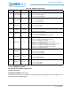
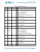
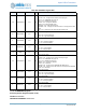
11.7.2.14CFGA Register
GPIO Configuration Register A (Pads 0-7)
OFFSET: 0x00000040
INSTANCE 0 ADDRESS: 0x40010040
GPIO configuration controls for GPIO[7:0]. Writes to this register must be unlocked by the PADKEY
register.
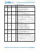
7:6 PAD48RSEL 0x0 RW
Pad 48 pullup resistor selection.
PULL1_5K = 0x0 - Pullup is ~1.5 KOhms
PULL6K = 0x1 - Pullup is ~6 KOhms
PULL12K = 0x2 - Pullup is ~12 KOhms
PULL24K = 0x3 - Pullup is ~24 KOhms
5:3 PAD48FNCSEL 0x3 RW
Pad 48 function select
UART0TX = 0x0 - Configure as the UART0 TX output signal
NCE48 = 0x1 - IOM/MSPI nCE group 48
CT28 = 0x2 - CTIMER conenction 28
GPIO48 = 0x3 - Configure as GPIO48
M5SCL = 0x4 - Configure as the IOMSTR5 I2C SCL clock I/O signal
M5SCK = 0x5 - Configure as the IOMSTR5 SPI SCK output
RSVD6 = 0x6 - Reserved
RSVD7 = 0x7 - Reserved
2 PAD48STRNG 0x0 RW
Pad 48 drive strength
LOW = 0x0 - Low drive strength
HIGH = 0x1 - High drive strength
1 PAD48INPEN 0x0 RW
Pad 48 input enable
DIS = 0x0 - Pad input disabled
EN = 0x1 - Pad input enabled
0 PAD48PULL 0x0 RW
Pad 48 pullup enable
DIS = 0x0 - Pullup disabled
EN = 0x1 - Pullup enabled
Table 651: CFGA Register
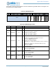
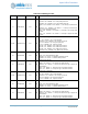
3
1
3
0
2
9
2
8
2
7
2
6
2
5
2
4
2
3
2
2
2
1
2
0
1
9
1
8
1
7
1
6
1
5
1
4
1
3
1
2
1
1
1
0
0
9
0
8
0
7
0
6
0
5
0
4
0
3
0
2
0
1
0
0
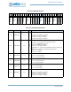
GPIO7INTD
GPIO7OUTCFG
GPIO7INCFG
GPIO6INTD
GPIO6OUTCFG
GPIO6INCFG
GPIO5INTD
GPIO5OUTCFG
GPIO5INCFG
GPIO4INTD
GPIO4OUTCFG
GPIO4INCFG
GPIO3INTD
GPIO3OUTCFG
GPIO3INCFG
GPIO2INTD
GPIO2OUTCFG
GPIO2INCFG
GPIO1INTD
GPIO1OUTCFG
GPIO1INCFG
GPIO0INTD
GPIO0OUTCFG
GPIO0INCFG
Table 650: PADREGM Register Bits
Bit Name Reset RW Description