
User Manual


Apollo3 Blue Datasheet
DS-A3-0p9p1 Page 439 of 909 2019 Ambiq Micro, Inc.
All rights reserved.
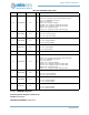
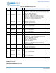
11.7.2.10PADREGJ Register
Pad Configuration Register J (Pads 36-39)
OFFSET: 0x00000024
INSTANCE 0 ADDRESS: 0x40010024
This register controls the pad configuration controls for PAD39 through PAD36. Writes to this register must
be unlocked by the PADKEY register.
1 PAD32INPEN 0x0 RW
Pad 32 input enable
DIS = 0x0 - Pad input disabled
EN = 0x1 - Pad input enabled
0 PAD32PULL 0x0 RW
Pad 32 pullup enable
DIS = 0x0 - Pullup disabled
EN = 0x1 - Pullup enabled
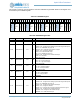
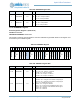
Table 643: PADREGJ Register
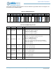
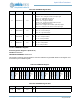
3
1
3
0
2
9
2
8
2
7
2
6
2
5
2
4
2
3
2
2
2
1
2
0
1
9
1
8
1
7
1
6
1
5
1
4
1
3
1
2
1
1
1
0
0
9
0
8
0
7
0
6
0
5
0
4
0
3
0
2
0
1
0
0
PAD39RSEL
PAD39FNC-
SEL
PAD39STRNG
PAD39INPEN
PAD39PULL
RSVD
PAD38FNC-
SEL
PAD38STRNG
PAD38INPEN
PAD38PULL
PAD37PWRDN
RSVD
PAD37FNC-
SEL
PAD37STRNG
PAD37INPEN
PAD37PULL
RSVD
PAD36PWRUP
PAD36FNC-
SEL
PAD36STRNG
PAD36INPEN
PAD36PULL
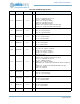
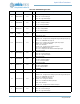
Table 644: PADREGJ Register Bits
Bit Name Reset RW Description
31:30 PAD39RSEL 0x0 RW
Pad 39 pullup resistor selection.
PULL1_5K = 0x0 - Pullup is ~1.5 KOhms
PULL6K = 0x1 - Pullup is ~6 KOhms
PULL12K = 0x2 - Pullup is ~12 KOhms
PULL24K = 0x3 - Pullup is ~24 KOhms
29:27 PAD39FNCSEL 0x3 RW
Pad 39 function select
UART0TX = 0x0 - Configure as the UART0 TX output signal
UART1TX = 0x1 - Configure as the UART1 TX output signal
CT25 = 0x2 - CTIMER connection 25
GPIO39 = 0x3 - Configure as GPIO39
M4SCL = 0x4 - Configure as the IOMSTR4 I2C SCL signal
M4SCK = 0x5 - Configure as the IOMSTR4 SPI SCK signal
RSVD6 = 0x6 - Reserved
RSVD7 = 0x7 - Reserved
Table 642: PADREGI Register Bits
Bit Name Reset RW Description