
User Manual


Apollo3 Blue Datasheet
DS-A3-0p9p1 Page 432 of 909 2019 Ambiq Micro, Inc.
All rights reserved.
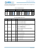
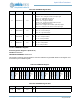
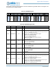
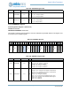
This register controls the pad configuration controls for PAD27 through PAD24. Writes to this register must
be unlocked by the PADKEY register.
Table 637: PADREGG Register
3
1
3
0
2
9
2
8
2
7
2
6
2
5
2
4
2
3
2
2
2
1
2
0
1
9
1
8
1
7
1
6
1
5
1
4
1
3
1
2
1
1
1
0
0
9
0
8
0
7
0
6
0
5
0
4
0
3
0
2
0
1
0
0
PAD27RSEL
PAD27FNC-
SEL
PAD27STRNG
PAD27INPEN
PAD27PULL
RSVD
PAD26FNC-
SEL
PAD26STRNG
PAD26INPEN
PAD26PULL
PAD25RSEL
PAD25FNC-
SEL
PAD25STRNG
PAD25INPEN
PAD25PULL
RSVD
PAD24FNC-
SEL
PAD24STRNG
PAD24INPEN
PAD24PULL
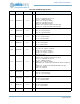
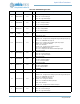
Table 638: PADREGG Register Bits
Bit Name Reset RW Description
31:30 PAD27RSEL 0x0 RW
Pad 27 pullup resistor selection.
PULL1_5K = 0x0 - Pullup is ~1.5 KOhms
PULL6K = 0x1 - Pullup is ~6 KOhms
PULL12K = 0x2 - Pullup is ~12 KOhms
PULL24K = 0x3 - Pullup is ~24 KOhms
29:27 PAD27FNCSEL 0x3 RW
Pad 27 function select
UART0RX = 0x0 - Configure as UART0 RX input signal
NCE27 = 0x1 - IOM/MSPI nCE group 27
CT5 = 0x2 - CTIMER connection 5
GPIO27 = 0x3 - Configure as GPIO27
M2SCL = 0x4 - Configure as I2C clock I/O signal from IOMSTR2
M2SCK = 0x5 - Configure as SPI clock output signal from IOMSTR2
RSVD6 = 0x6 - Reserved
RSVD7 = 0x7 - Reserved
26 PAD27STRNG 0x0 RW
Pad 27 drive strength
LOW = 0x0 - Low drive strength
HIGH = 0x1 - High drive strength
25 PAD27INPEN 0x0 RW
Pad 27 input enable
DIS = 0x0 - Pad input disabled
EN = 0x1 - Pad input enabled
24 PAD27PULL 0x0 RW
Pad 27 pullup enable
DIS = 0x0 - Pullup disabled
EN = 0x1 - Pullup enabled
23:22 RSVD 0x0 RO
RESERVED