
User Manual


Apollo3 Blue Datasheet
DS-A3-0p9p1 Page 431 of 909 2019 Ambiq Micro, Inc.
All rights reserved.
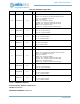
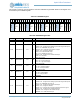
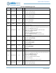
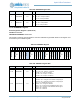
11.7.2.7 PADREGG Register
Pad Configuration Register G (Pads 24-27)
OFFSET: 0x00000018
INSTANCE 0 ADDRESS: 0x40010018
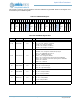
13:11 PAD21FNCSEL 0x0 RW
Pad 21 function select
SWDIO = 0x0 - Configure as the serial wire debug data signal
NCE21 = 0x1 - IOM/MSPI nCE group 21
RSVD = 0x2 - Reserved
GPIO21 = 0x3 - Configure as GPIO21
UART0RX = 0x4 - Configure as UART0 RX input signal
UART1RX = 0x5 - Configure as UART1 RX input signal
I2SBCLK = 0x6 - I2S byte clock input
UA1CTS = 0x7 - Configure as UART1 CTS input signal
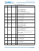
10 PAD21STRNG 0x0 RW
Pad 21 drive strength
LOW = 0x0 - Low drive strength
HIGH = 0x1 - High drive strength
9 PAD21INPEN 0x1 RW
Pad 21 input enable
DIS = 0x0 - Pad input disabled
EN = 0x1 - Pad input enabled
8 PAD21PULL 0x0 RW
Pad 21 pullup enable
DIS = 0x0 - Pullup disabled
EN = 0x1 - Pullup enabled
7:6 RSVD 0x0 RO
RESERVED
5:3 PAD20FNCSEL 0x0 RW
Pad 20 function select
SWDCK = 0x0 - Configure as the serial wire debug clock signal
NCE20 = 0x1 - IOM/MSPI nCE group 20
RSVD = 0x2 - Reserved
GPIO20 = 0x3 - Configure as GPIO20
UART0TX = 0x4 - Configure as UART0 TX output signal
UART1TX = 0x5 - Configure as UART1 TX output signal
I2SBCLK = 0x6 - I2S byte clock input
UA1RTS = 0x7 - Configure as UART1 RTS output signal
2 PAD20STRNG 0x0 RW
Pad 20 drive strength
LOW = 0x0 - Low drive strength
HIGH = 0x1 - High drive strength
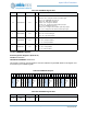
1 PAD20INPEN 0x1 RW
Pad 20 input enable
DIS = 0x0 - Pad input disabled
EN = 0x1 - Pad input enabled
0 PAD20PULL 0x0 RW
Pad 20 pulldown enable
DIS = 0x0 - Pulldown disabled
EN = 0x1 - Pulldown enabled
Table 636: PADREGF Register Bits
Bit Name Reset RW Description