
User Manual


Apollo3 Blue Datasheet
DS-A3-0p9p1 Page 428 of 909 2019 Ambiq Micro, Inc.
All rights reserved.
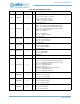
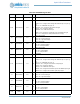
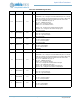
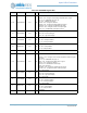
21:19 PAD18FNCSEL 0x3 RW
Pad 18 function select
CMPIN1 = 0x0 - Configure as the analog comparator input 1 signal
NCE18 = 0x1 - IOM/MSPI nCE group 18
CT4 = 0x2 - CTIMER connection 4
GPIO18 = 0x3 - Configure as GPIO18
UA0RTS = 0x4 - Configure as UART0 RTS output signal
ANATEST2 = 0x5 - Configure as ANATEST2 I/O signal
UART1TX = 0x6 - Configure as UART1 TX output signal
SCCIO = 0x7 - SCARD data input/output connectin
18 PAD18STRNG 0x0 RW
Pad 18 drive strength
LOW = 0x0 - Low drive strength
HIGH = 0x1 - High drive strength
17 PAD18INPEN 0x0 RW
Pad 18 input enable
DIS = 0x0 - Pad input disabled
EN = 0x1 - Pad input enabled
16 PAD18PULL 0x0 RW
Pad 18 pullup enable
DIS = 0x0 - Pullup disabled
EN = 0x1 - Pullup enabled
15:14 RSVD 0x0 RO
RESERVED
13:11 PAD17FNCSEL 0x3 RW
Pad 17 function select
CMPRF1 = 0x0 - Configure as the analog comparator reference signal 1
input signal
NCE17 = 0x1 - IOM/MSPI nCE group 17
TRIG1 = 0x2 - Configure as the ADC Trigger 1 signal
GPIO17 = 0x3 - Configure as GPIO17
SCCCLK = 0x4 - SCARD serial clock output
RSVD = 0x5 - Reserved
UART0RX = 0x6 - Configure as UART0 RX input signal
UA1CTS = 0x7 - Configure as UART1 CTS input signal
10 PAD17STRNG 0x0 RW
Pad 17 drive strength
LOW = 0x0 - Low drive strength
HIGH = 0x1 - High drive strength
9 PAD17INPEN 0x0 RW
Pad 17 input enable
DIS = 0x0 - Pad input disabled
EN = 0x1 - Pad input enabled
8 PAD17PULL 0x0 RW
Pad 17 pullup enable
DIS = 0x0 - Pullup disabled
EN = 0x1 - Pullup enabled
7:6 RSVD 0x0 RO
RESERVED
Table 634: PADREGE Register Bits
Bit Name Reset RW Description