
User Manual


Apollo3 Blue Datasheet
DS-A3-0p9p1 Page 420 of 909 2019 Ambiq Micro, Inc.
All rights reserved.
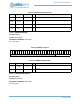
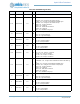
Table 628: PADREGB Register Bits
Bit Name Reset RW Description
31:30 RSVD 0x0 RO
RESERVED
29:27 PAD7FNCSEL 0x3 RW
Pad 7 function select
NCE7 = 0x0 - IOM/MSPI nCE group 7
M0MOSI = 0x1 - Configure as the IOMSTR0 SPI MOSI signal
CLKOUT = 0x2 - Configure as the CLKOUT signal
GPIO7 = 0x3 - Configure as GPIO7
TRIG0 = 0x4 - Configure as the ADC Trigger 0 signal
UART0TX = 0x5 - Configure as the UART0 TX output signal
RSVD = 0x6 - Reserved
CT19 = 0x7 - CTIMER connection 19
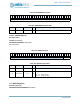
26 PAD7STRNG 0x0 RW
Pad 7 drive strength
LOW = 0x0 - Low drive strength
HIGH = 0x1 - High drive strength
25 PAD7INPEN 0x0 RW
Pad 7 input enable
DIS = 0x0 - Pad input disabled
EN = 0x1 - Pad input enabled
24 PAD7PULL 0x0 RW
Pad 7 pullup enable
DIS = 0x0 - Pullup disabled
EN = 0x1 - Pullup enabled
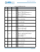
23:22 PAD6RSEL 0x0 RW
Pad 6 pullup resistor selection.
PULL1_5K = 0x0 - Pullup is ~1.5 KOhms
PULL6K = 0x1 - Pullup is ~6 KOhms
PULL12K = 0x2 - Pullup is ~12 KOhms
PULL24K = 0x3 - Pullup is ~24 KOhms
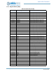
21:19 PAD6FNCSEL 0x3 RW
Pad 6 function select
M0SDAWIR3 = 0x0 - Configure as the IOMSTR0 I2C SDA or SPI WIR3 sig-
nal
M0MISO = 0x1 - Configure as the IOMSTR0 SPI MISO signal
UA0CTS = 0x2 - Configure as the UART0 CTS input signal
GPIO6 = 0x3 - Configure as GPIO6
RSVD4 = 0x4 - Reserved
CT10 = 0x5 - CTIMER connection 10
RSVD6 = 0x6 - Reserved
I2S_DAT = 0x7 - Configure as the PDM I2S Data output signal
18 PAD6STRNG 0x0 RW
Pad 6 drive strength
LOW = 0x0 - Low drive strength
HIGH = 0x1 - High drive strength
17 PAD6INPEN 0x0 RW
Pad 6 input enable
DIS = 0x0 - Pad input disabled
EN = 0x1 - Pad input enabled
16 PAD6PULL 0x0 RW
Pad 6 pullup enable
DIS = 0x0 - Pullup disabled
EN = 0x1 - Pullup enabled