
User Manual

Apollo3 Blue Datasheet
DS-A3-0p9p1 Page 408 of 909 2019 Ambiq Micro, Inc.
All rights reserved.
11.5.13Implementing the Software Debug Port Connections
The software debug clock (SWDCK) and data (SWDIO) must be connected on pads 20 and 21
respectively. PAD20FNCSEL and PAD21FNCSEL must be set to 0, PAD20INPEN and PAD21INPEN must
be set, and PAD20PULL and PAD21PULL must be set, which results in a default state of SWDCK low and
SWDIO high. Pads 14 and 15 can alternatively be used for SWDCK and SWDIO functionality, respectively.
These pads are, however, not selected by default. Using pads 14 and 15 requires PAD14FNCSEL to be
set to 6 and PAD15FNCSEL to be set to 6, PAD14INPEN and PAD15INPEN to be set, and PAD14PULL
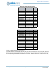
and PAD15PULL to be set. The optional continuous output signal SWO may be configured on a variety of
pads as shown in Table 612, and PADnINPEN and PADnPULL should be cleared for the selected pad.
11.5.14Fast GPIO
11.5.14.1Description
Access to GPIO pin registers on the Apollo3 Blue MCU can be multiple CPU cycles to complete. To
support certain functions that require shorter latency access, a fast GPIO interface is supported. The fast
GPIO is accessed via the fast GPIO registers shown in the next section.
11.6 FASTGPIO Registers
APB DMA Register Interfaces
INSTANCE 0 BASE ADDRESS:0x40011000
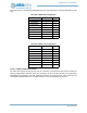
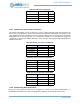
PAD18FNCSEL 0 CMPIN1 18
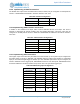
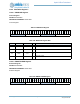
Table 612: SWO Configuration
Field Value Pad
PAD15FNCSEL 7 15
PAD22FNCSEL 7 22
PAD24FNCSEL 7 24
PAD33FNCSEL 7 33
PAD41FNCSEL 2 41
PAD45FNCSEL 7 45
PAD46FNCSEL 7 46
Table 611: Voltage Comparator Input Configuration
Field Value Input Pad