
User Manual

Apollo3 Blue Datasheet
DS-A3-0p9p1 Page 407 of 909 2019 Ambiq Micro, Inc.
All rights reserved.
I
11.5.12mplementing Voltage Comparator Connections
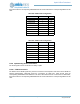
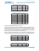
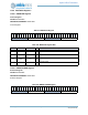
Two types of pad connections may be made for the Voltage Comparator (VCOMP) module. Three
reference voltages may be used for the comparator negative input as shown in Table 610. The voltage to
be applied to the comparator positive input are shown in . In each case PADnINPEN and PADnPULL
should be clearedNote that for CMPRF2, this pin is muxed with ADCSE6 allowing for the same reference
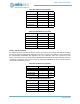
input to be used for both ADC and VCOMP operations. Additionally, CMPIN0 is muxed with ADCSE0
allowing for the same input to be used for both ADC and VCOMP operations.
NOTE: if voltage comparator and ADC operation are concurrently sampling the CMPIN0/ADCSE0 input,
quality of the sample may be degraded and cannot be guaranteed. It is recommended that voltage
comparator and ADC operations are sampled independently (time sliced) to avoid any signal quality loss.
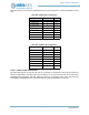
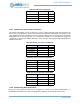
PAD12FNCSEL 0
ADCD0P/
SE9
12
PAD14FNCSEL 0 ADCD1P 14
PAD15FNCSEL 0 ADCD1M 15
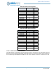
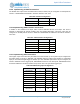
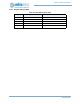
Table 609: ADC Trigger Input Configuration
Field Value Input Pad
PAD7FNCSEL 4 TRIG0 7
PAD16FNCSEL 2 TRIG0 16
PAD40FNCSEL 2 TRIG0 40
PAD3FNCSEL 6 TRIG1 3
PAD17FNCSEL 2 TRIG1 17
PAD36FNCSEL 0 TRIG1 36
PAD37FNCSEL 0 TRIG2 37
PAD38FNCSEL 0 TRIG3 38
Table 610: Voltage Comparator Reference Configuration
Field Value Input Pad
PAD19FNCSEL 0 CMPRF0 19
PAD17FNCSEL 0 CMPRF1 17
PAD34FNCSEL 4 CMPRF2 34
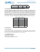
Table 611: Voltage Comparator Input Configuration
Field Value Input Pad
PAD16FNCSEL 5 CMPIN0 16
Table 608: ADC Analog Input Configuration
Field Value Input Pad