
User Manual


Apollo3 Blue Datasheet
DS-A3-0p9p1 Page 389 of 909 2019 Ambiq Micro, Inc.
All rights reserved.
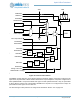
11.4.3 Input Control
The input circuitry of the pad may be disabled by clearing the PADnINPEN bit. This configuration should
always be set if the pad input is not being used, as it prevents unnecessary current consumption if the pad
voltage happens to float to a level between VDD and Ground. If PADnINPEN is 0, the pad will always read
as a 0.
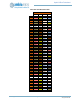
If PADnINPEN is set, the pad input then goes to two places. It is driven to the selected module signal as
selected in Table 559. In addition, the pad input can always be read from the GPIORD register unless the
pad is configured as a GPIO (PADnFNCSEL = 0x3) and GPIOnINCFG is high, which will force the
GPIORD input to be a zero. The ability to always read the pad value is very useful in some diagnostic
cases.
The pad input is always sent to the GPIO interrupt logic, and a pad transition in the direction selected by
GPIOnINTD will set the corresponding GPIOn_INT flip-flop. Note that this interrupt will be set even if the
pad is not configured as a GPIO, which may be useful in detecting functions. As an example, this could be
used to generate an interrupt when the I
2
C/SPI Slave nCE signal is driven low by the Interface Host.
11.4.4 Pull-up Control
If PADnPULL is high, a pullup resistor is connected between the pad and VDDH, except for pad 20, where
PADnPULL connects the resistor to VSS rather than VDDH.
The fourteen pads which can be I
2
C/SPI Master output drivers (pads 0, 1, 5, 6, 8, 9, 25, 27, 39, 40, 42, 43
48 and 49) contain the additional circuitry shown with the dashed lines. In this case four different pullup
resistors are selected by the PADnRSEL field.
11.4.5 Analog Pad Configuration
Pads which may have analog connections (pads 11-19, 29 and 31-35) include the circuitry shown with the
dotted lines. If the pad is configured in analog mode (reference the analog input function selections in
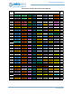
Table 1: Pin List and Function Table, the pad is connected directly to the particular analog module signal. In
addition, OUTENSEL is forced high to disable the pad output, and the input of the pad is disabled
independent of the value of PADnINPEN.
11.5 Module-specific Pad Configuration
The following sections describe in detail how to configure the pads for each module function.
11.5.1 Implementing IO Master Connections
The six IO Master modules must be correctly connected to the appropriate pads in order to operate.
11.5.1.1 IO Master 0 I
2
C Connection
I
2
C mode of IO Master 0 uses pad 5 as SCL and pad 6 as SDA. This mode is configured by setting the
PADnFNCSEL fields as shown in Table 566. The PAD5INPEN and PAD6INPEN bits must be set. If the
internal I
2
C pullup resistors are to be used, PAD5PULL and PAD6PULL should be set, and the PAD5RSEL