
User Manual


Apollo3 Blue Datasheet
DS-A3-0p9p1 Page 387 of 909 2019 Ambiq Micro, Inc.
All rights reserved.
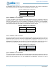
Below describes the interrupt configuration.
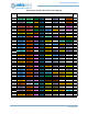
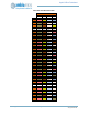
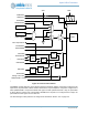
11.4 Pad Connection Summary
Figure 62 shows the detailed implementation of each pad. Each element will be described in detail.
11.4.1 Output Selection
There is a multiplexer which selects the module signal to be driven to the output based on
REG_GPIO_PADREGy_PADnFNCSEL field. This implements the multiplexing shown in Table 559 for
output pads. For all pads, a PADnFNCSEL value of 0x3 selects the value in the corresponding GPIO_WTy
register bit.
Certain functional groups, Timer (CT), NCE and MSPI in particular, have additional pre-muxing
configuration as noted.
NOTE: In order to achieve high data rates on the MSPI interface, some of the normal GPIO muxing has
been bypassed. When MSPI-related pads (24, 22, 26, 4, 23, 0, 1, 2, 3) are used for non-MSPI functions,
the MSPI module must be powered down or the related bit in the MSPI PADOUTEN register must be
disabled to ensure that the MSPI does not drive data to the pad (which is logically OR'd with the data from
the GPIO functional mux select).
11.4.2 Output Control
The pad driver for each pad has a data input and an output enable input. Each of these controls is selected
from among several alternatives based on the OUTDATSEL and OUTENSEL signals which are controlled
by the selection of the output type as shown in Table 562 and Table 563.
OUTDATSEL normally selects the data from the output multiplexer, but if the pad is configured as Open
Drain the data input is selected to be low.
Table 565: Interrupt Configuration
INCFG INTD Interrupt
0 0 Low -> high transition
0 1 High -> low transition
1 0 Disabled
1 1 Either low -> high or high -> low transition