
User Manual


Apollo3 Blue Datasheet
DS-A3-0p9p1 Page 386 of 909 2019 Ambiq Micro, Inc.
All rights reserved.
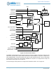
11.3 General Purpose I/O (GPIO) Functions
For each pad, if the PADnFNCSEL field is set to 0x3 the pad is connected to the corresponding GPIO
signal. This section describes the configuration functions specific to GPIO pads.
11.3.1 Configuring the GPIO Functions
Each GPIO must be configured in the REG_GPIO_CFGy (y = A to G) Registers as an input and/or output.
Note that the PADKEY Register must be set to the value 0x73 in order to write the REG_GPIO_CFGy
Registers. Each output may be push-pull, open drain, disabled, or tri-stated as selected by the
REG_GPIO_CFGy_GPIOnOUTCFG field. If the output is configured as push-pull, the pad will be driven
with the corresponding bit in the REG_GPIO_WTy (y = A or B) Register. If the output is configured as open
drain, the pad will be pulled low if the corresponding bit in the WTy Register is a 0, and will be floating if the
corresponding bit in the WTy Register is a 1. If the output is configured as tri-state, the pad will be driven
with the corresponding bit in the WTy Register if the corresponding bit in the REG_GPIO_ENy Register is
a 1. If the bit in ENy is a 0, the output will be floating.
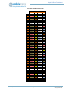
For Apollo3 Blue MCU, if the PADxFNCSEL is set to a “NCE” signal group, the additional NCE encoding is
applied as shown in Table 564 based on GPIOxOUTCFG and the pad is automatically configured for push-
pull output. If the PADxFNCSEL is set to a “MSPI” signal group, the additional MSPI encoding is applied as
shown in Section 11.5.2.
11.3.2 Reading from a GPIO Pad
All GPIO inputs are readable at all times unless the interrupt configuration (determined by
REG_GPIO_CFGy_GPIOnINCFG and REG_GPIO_CFGy_GPIOnINTD) is set to “disabled”, even if the
pad is not configured as a GPIO. The current values of pads 0 to 31 are read in the REG_GPIO_RDA
Register, and the current values of pads 32 to 49 are read in the REG_GPIO_RDB Register. If the
REG_GPIO_CFGy_GPIOnINCFG bit is set for a GPIO, it will always read as zero if the interrupt
configuration is set to “disabled”.
11.3.3 Writing to a GPIO Pad
The GPIO pad outputs are controlled by the REG_GPIO_WTA/B Registers and the REG_GPIO_ENA/B
Registers. Each of these registers may be directly written and read. Because each GPIO is often an
independent function, the capability also exists to set or clear one or more bits without having to perform a
read-modify-write operation. If the REG_GPIO_WTSA or REG_GPIO_WTSB Register is written, the
corresponding bit in WTA/B will be set if the write data is 1, otherwise the WTA/B bit will not be changed. If
the REG_GPIO_WTCA or REG_GPIO_WTCB Register is written, the corresponding bit in WTA/B will be
cleared if the write data is 1, otherwise the WTA/B bit will not be changed.
If a GPIO pad is configured for tri-state output mode, the ENA/B Register controls the enabling of each bit.
ENA and ENB may be directly written, and individual bits may be set or cleared by writing the ENSA/B or
ENCA/B Registers with a 1 in the desired bit position.
11.3.4 GPIO Interrupts
Each GPIO pad can be configured to generate an interrupt on a high-to-low transition or a low-to-high or
either transition, as selected by the REG_GPIO_CFGy_GPIOnINTD and
REG_GPIO_CFGy_GPIOnINCFG bits. This interrupt will be generated even if the pad is not configured as
a GPIO in the Pad Configuration logic. Each interrupt is enabled, disabled, cleared or set with a standard
set of Interrupt Registers GPIOA_IER, GPIOA_ISR, GPIOA_WCR and GPIOB_WSR for GPIO pads 0 to
31, and Registers GPIOB_IER, GPIOB_ISR, GPIOB_WCR and GPIOB_WSR for GPIO pads 32 to 49.