
User Manual

Apollo3 Blue Datasheet
DS-A3-0p9p1 Page 379 of 909 2019 Ambiq Micro, Inc.
All rights reserved.
11. GPIO and Pad Configuration Module
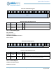
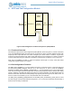
Figure 61. Block diagram for the General Purpose I/O (GPIO) Module
11.1 Functional Overview
The General Purpose I/O and Pad Configuration (GPIO) Module, shown in Figure 61, controls connections
to up to 50 digital/analog pads. Each pad may be connected to a variety of module interface signals, with
all pad input and output selection and control managed by the GPIO module. In addition, any pad may
function as a general purpose input and/or output pad which may be configured for a variety of external
functions. Each GPIO may be configured to generate an interrupt when a transition occurs on the input.
Note: Once the PADKEY is written, it should be explicitly cleared (with a non-key value) after GPIO
configuration register updates are complete.
11.2 Pad Configuration Functions
The REG_GPIO_PADREGy (y = A to M) registers are used to control the function of each pad. Note that
the REG_GPIO_PADKEY Register must be set to the value 0x73 in order to write the PADREGn
Registers. The REG_GPIO_PADREGy_PADnFNCSEL (n = 0 to 49) field selects one of up to eight signals
to be used for each pad, as shown in Table 559. Functions are grouped by module, with the color coding
shown in Table 561. This table also defines the pad type for each configuration. The Special pad types are
defined in Table 562. Note that the CSP package only supports pads 0 through 23, 26, 28-29, 39-41, 44
and 47-49, which are indicated by an ‘X’ in the CSP PKG column of Table 559.
The REG_GPIO_PADREGy_PADnSTRNG bit and the REG_GPIO_ALTPADCFGy_PADn_DS1 bit control
the drive strength of the pad. Nominal drive strengths of 2, 4, 8 or 12 mA can be selected with the setting of
these two bits according to Table 558.
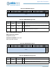
Bus
Interface
GPIO
REGs
Config
Registers
Pad Muxes
IO Pads
Controller IO