
User Manual

Apollo3 Blue Datasheet
DS-A3-0p9p1 Page 336 of 909 2019 Ambiq Micro, Inc.
All rights reserved.
9.9.10 General Address Detection
The I
2
C/SPI Slave may be configured to detect an I
2
C General Address (0x00) write. If this address is
detected, the first data byte written is stored in the REG_IOSLAVE_GADATA Register and the GENAD
interrupt flag is set. This allows software to create the appropriate response, which is typically to reset the
I
2
C/SPI Slave.
9.10 SPI Interface
The I
2
C/SPI Slave includes a standard 3-wire or 4-wire SPI interface. The serial peripheral interface (SPI)
bus is intended for synchronous communication between different ICs. 4-wire SPI consists of four signal
lines: serial data input (MOSI), serial data output (MISO), serial clock (SCL) and an active low chip enable
(nCE). The I
2
C/SPI Slave may be connected to a master with a 3-wire SPI interface by configuring 3-wire
mode in the pin configuration block of the GPIO module, which will tie MOSI and MISO together. By
definition, a device that sends a message is called the “transmitter”, and the device that accepts the
message is called the “receiver”. The device that controls the message transfer by driving SCL is called
“master”. The devices that are controlled by the master are called “slaves”. The I
2
C/SPI Slave SPI Slave is
always a slave device.
The nCE input is used to initiate and terminate a data transfer. The SCL input is used to synchronize data
transfer between the master and the slave devices via the MOSI (master to slave) and MISO (slave to
master) lines. The SCL input, which is generated by the master, is active only during address and data
transfer to any device on the SPI bus.
The I
2
C/SPI Slave supports clock frequencies up to 12 MHz, and responds to all SPI configurations of
CPOL and CPHA using the SPOL configuration bit. There is one clock for each bit transferred. Address
and data bits are transferred in groups of eight bits.
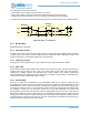
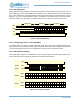
9.10.1 Write Operation
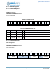
Figure 52 shows a SPI write operation. The operation is initiated when the nCE signal to the Apollo3 Blue
MCU goes low. At that point an 8-bit Address byte is transmitted from the master on the MOSI line, with the
upper RW bit indicating read (if 0) or write (if 1). In this example the RW bit is a one selecting a write
operation, and the lower 7 bits of the Address byte contain the Offset Address, which is loaded into the
Address Pointer of the I
2
C/SPI Slave.
Each subsequent byte is loaded into the register selected by the Address Pointer, and the Address Pointer
is incremented. The operation is terminated by the master by bringing the nCE signal high. Note that the
MISO line is not used in a write operation and is held in the high impedance state by the I
2
C/SPI Slave.
Note also that if the Address Pointer is 0x7F, it does not increment on the read.
Figure 52. SPI Write Operation
W 6 1
MOSI
SCK
0 7 6 1 0
Offset Address
nCE
X
Data Byte N
7 6 1 0
Data Byte N+1
X
MISO
5 4 3 2 5 4 3 2 5 4 3 2