
User Manual


Apollo3 Blue Datasheet
DS-A3-0p9p1 Page 325 of 909 2019 Ambiq Micro, Inc.
All rights reserved.
9. I
2
C/SPI Slave Module
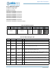
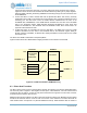
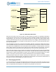
Figure 42. Block diagram for the I
2
C/SPI Slave Module
9.1 Functional Overview
The I
2
C/SPI Slave Module, shown in Figure 42, allows the Apollo3 Blue MCU to function as a Slave in an
I
2
C or SPI system. The I
2
C/SPI Slave operates in an independent fashion, so that the Apollo3 Blue MCU
may be placed in a sleep mode and still receive operations over the I/O interface. The Slave may be
configured to generate an interrupt on specific references.
The I
2
C/SPI Slave contains 256 bytes of RAM which is only accessible when the module is enabled. This
RAM may be flexibly configured into three spaces: a block directly accessible via the I/O interface, a block
which functions as a FIFO for read operations on the interface, and a block of generally accessible RAM
used to store parameters during deep sleep mode.
In I
2
C mode the Slave supports fully configurable 7 and 10-bit addressing with interface timing limits as
specified in Table 1155. In SPI mode, the Slave supports all polarity/phase combinations and interface
frequencies as specified in Table 1156.
9.2 Local RAM Allocation
The I
2
C/SPI Slave is built around a 256-byte local RAM (LRAM), through which all data flows between the
CPU AHB and the IO interface. The I
2
C/SPI Slave supports a 128-byte offset space when accessed from
the I/O interface.
The LRAM is divided into three separate areas on 8-byte boundaries. These areas are:
1. A Direct Area for direct communication between the host and the MCU, which is mapped between
the AHB address space and the I/O address space. This area is from LRAM address 0x00 to the
address calculated from the 5-bit FIFOBASE field in the FIFO configuration register (FIFOCFG),
minus 1. This 5-bit field (REG_IOSLAVE_FIFOCFG_FIFOBASE) should contain a value that rep-
Bus
Interface
REGs
INTs
SPI Slave Controller
I
2
C Slave Controller
FIFO
IO Mux