
User Manual


Apollo3 Blue Datasheet
DS-A3-0p9p1 Page 324 of 909 2019 Ambiq Micro, Inc.
All rights reserved.
8.15.2.36IOMDBG Register
IOM Debug Register
OFFSET: 0x00000410
INSTANCE 0 ADDRESS: 0x50004410
INSTANCE 1 ADDRESS: 0x50005410
INSTANCE 2 ADDRESS: 0x50006410
INSTANCE 3 ADDRESS: 0x50007410
INSTANCE 4 ADDRESS: 0x50008410
INSTANCE 5 ADDRESS: 0x50009410
Debug control
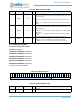
9:0 DEVADDR 0x0 RW
I2C address of the device that the Master will use to target for read/write
operations. This can be either a 7b or 10b address.
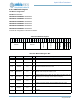
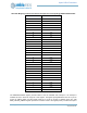
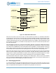
Table 466: IOMDBG Register
3
1
3
0
2
9
2
8
2
7
2
6
2
5
2
4
2
3
2
2
2
1
2
0
1
9
1
8
1
7
1
6
1
5
1
4
1
3
1
2
1
1
1
0
0
9
0
8
0
7
0
6
0
5
0
4
0
3
0
2
0
1
0
0
DBGDATA
APBCLKON
IOCLKON
DBGEN
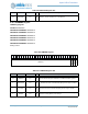
Table 467: IOMDBG Register Bits
Bit Name Reset RW Description
31:3 DBGDATA 0x0 RW
Debug control for various options. DBGDATA[1:0] is used to select
between different debug data available in the DBG0 and DBG1 registers.
2 APBCLKON 0x0 RW
APBCLK debug clock control. Enable APB_CLK to be active when this bit is
'1'. Otherwise, the clock is controlled with gating from the logic as needed.
1 IOCLKON 0x0 RW
IOCLK debug clock control. Enable IO_CLK to be active when this bit is '1'.
Otherwise, the clock is controlled with gating from the logic as needed.
0 DBGEN 0x0 RW
Debug Enable. Setting bit will enable the update of data within this register,
otherwise it is clock gated for power savings
Table 465: DEVCFG Register Bits
Bit Name Reset RW Description