
User Manual


Apollo3 Blue Datasheet
DS-A3-0p9p1 Page 322 of 909 2019 Ambiq Micro, Inc.
All rights reserved.
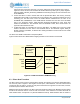
8.15.2.34MI2CCFG Register
I2C Master configuration
OFFSET: 0x00000400
INSTANCE 0 ADDRESS: 0x50004400
INSTANCE 1 ADDRESS: 0x50005400
INSTANCE 2 ADDRESS: 0x50006400
INSTANCE 3 ADDRESS: 0x50007400
INSTANCE 4 ADDRESS: 0x50008400
INSTANCE 5 ADDRESS: 0x50009400
Controls the configuration of the I2C bus master.
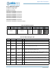
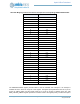
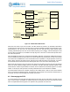
Table 462: MI2CCFG Register
3
1
3
0
2
9
2
8
2
7
2
6
2
5
2
4
2
3
2
2
2
1
2
0
1
9
1
8
1
7
1
6
1
5
1
4
1
3
1
2
1
1
1
0
0
9
0
8
0
7
0
6
0
5
0
4
0
3
0
2
0
1
0
0
RSRVD3
STRDIS
SMPCNT
SDAENDLY
SCLENDLY
RSRVD2
MI2CRST
SDADLY
RSRVD1
ARBEN
I2CLSB
ADDRSZ
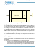
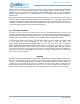
Table 463: MI2CCFG Register Bits
Bit Name Reset RW Description
31:25 RSRVD3 0x0 RO
Reserved
24 STRDIS 0x0 RW
Disable detection of clock stretch events smaller than 1 cycle
23:16 SMPCNT 0x0 RW
Number of Base clk cycles to wait before sampling the SCL clock to deter-
mine if a clock stretch event has occured
15:12 SDAENDLY 0x0 RW
Number of IOCLK cycles to delay the SDA output en (all transitions
affected). Used to delay data relative to clock
11:8 SCLENDLY 0x0 RW
Number of IOCLK cycles to delay the rising edge of the SCL output en
(clock will go low on this edge). Used to allow clock shaping.
7 RSRVD2 0x0 RO
Reserved
6 MI2CRST 0x0 RW
Not used. To reset the module, toggle the SMOD_EN for the module
5:4 SDADLY 0x0 RW
Delay to enable on the SDA output. Values are 0x0-0x3.
3 RSRVD1 0x0 RO
Reserved