
User Manual

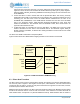

Apollo3 Blue Datasheet
DS-A3-0p9p1 Page 321 of 909 2019 Ambiq Micro, Inc.
All rights reserved.
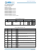
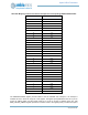
23 SPILSB 0x0 RW
Selects data transfer as MSB first (0) or LSB first (1) for the data portion of
the SPI transaction. The offset bytes are always transmitted MSB first.
MSB = 0x0 - Send and receive MSB bit first
LSB = 0x1 - Send and receive LSB bit first
22 RDFCPOL 0x0 RW
selects the read flow control signal polarity.
HIGH = 0x0 - Flow control signal high creates flow control.
LOW = 0x1 - Flow control signal low creates flow control.
21 WTFCPOL 0x1 RW
selects the write flow control signal polarity. The transfers are halted when
the selected flow control signal is OPPOSITE polarity of bit. (For example:
WTFCPOL = 0 will allow a IRQ=1 to pause transfers).
HIGH = 0x0 - Flow control signal high(1) creates flow control and byte trans-
fers will stop until the flow control signal goes low.
LOW = 0x1 - Flow control signal low(0) creates flow control and byte trans-
fers will stop until the flow control signal goes high(1).
20 WTFCIRQ 0x0 RW
selects the write mode flow control signal.
MISO = 0x0 - MISO is used as the write mode flow control signal.
IRQ = 0x1 - IRQ is used as the write mode flow control signal.
19 RSVD 0x0 RO
Reserved
18 MOSIINV 0x0 RW
inverts MOSI when flow control is enabled.
NORMAL = 0x0 - MOSI is set to 0 in read mode and 1 in write mode.
INVERT = 0x1 - MOSI is set to 1 in read mode and 0 in write mode.
17 RDFC 0x0 RW
enables read mode flow control.
DIS = 0x0 - Read mode flow control disabled.
EN = 0x1 - Read mode flow control enabled.
16 WTFC 0x0 RW
enables write mode flow control.
DIS = 0x0 - Write mode flow control disabled.
EN = 0x1 - Write mode flow control enabled.
15:3 RSVD 0x0 RO
RESERVED
2 FULLDUP 0x0 RW
Enables full duplex mode for Master SPI write operations. Data will be cap-
tured simultaneously into the read fifo
1 SPHA 0x0 RW
selects SPI phase.
SAMPLE_LEADING_EDGE = 0x0 - Sample on the leading (first) clock
edge.
SAMPLE_TRAILING_EDGE = 0x1 - Sample on the trailing (second) clock
edge.
0 SPOL 0x0 RW
selects SPI polarity.
CLK_BASE_0 = 0x0 - The base value of the clock is 0.
CLK_BASE_1 = 0x1 - The base value of the clock is 1.
Table 461: MSPICFG Register Bits
Bit Name Reset RW Description