
User Manual


Apollo3 Blue Datasheet
DS-A3-0p9p1 Page 310 of 909 2019 Ambiq Micro, Inc.
All rights reserved.
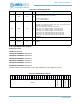
8.15.2.22DMATARGADDR Register
DMA Target Address Register
OFFSET: 0x0000028C
INSTANCE 0 ADDRESS: 0x5000428C
INSTANCE 1 ADDRESS: 0x5000528C
INSTANCE 2 ADDRESS: 0x5000628C
INSTANCE 3 ADDRESS: 0x5000728C
INSTANCE 4 ADDRESS: 0x5000828C
INSTANCE 5 ADDRESS: 0x5000928C
The source or destination address internal the SRAM for the DMA data. For write operations, this can
only be SRAM data (ADDR bit 28 = 1); For read operations, this can ve either SRAM or FLASH (ADDR bit
28 = 0)
11:0 TOTCOUNT 0x0 RW
Triggered DMA from Command complete event occured. Bit is read only
and can be cleared by disabling the DTHR trigger enable or by disabling
DMA.
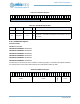
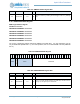
Table 438: DMATARGADDR Register
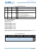
3
1
3
0
2
9
2
8
2
7
2
6
2
5
2
4
2
3
2
2
2
1
2
0
1
9
1
8
1
7
1
6
1
5
1
4
1
3
1
2
1
1
1
0
0
9
0
8
0
7
0
6
0
5
0
4
0
3
0
2
0
1
0
0
RSVD
TARGADDR28
RSVD TARGADDR
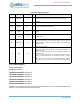
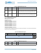
Table 439: DMATARGADDR Register Bits
Bit Name Reset RW Description
31:29 RSVD 0x0 RO
Reserved
28 TARGADDR28 0x0 RW
Bit 28 of the target byte address for source of DMA (either read or write). In
cases of non-word aligned addresses, the DMA logic will take care for
ensuring only the target bytes are read/written.
27:20 RSVD 0x0 RO
Reserved
Table 437: DMATOTCOUNT Register Bits
Bit Name Reset RW Description