
User Manual

Apollo3 Blue Datasheet
DS-A3-0p9p1 Page 275 of 909 2019 Ambiq Micro, Inc.
All rights reserved.
SPI operations may transfer up to 4095 bytes in a single transfer, as the TSIZE field in the CMD register
provides a 12-bit length specification.
8.8.2 SPI Slave Addressing
In SPI mode, the Command specifies the slave channel to be used in theCMDSEL field. The I
2
C/SPI
Master supports up to four slaves, each of which has its own nCE signal which can be configured on an IO
pin. Additional slaves may be supported using GPIO pins and external decoding.
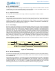
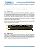
8.8.3 SPI Normal Write
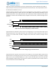
Figure 32 shows the case of a SPI Normal Write operation selected in the OPER field. The operation is
initiated when the I
2
C/SPI Master pulls one of the four nCE signals low. At that point the I
2
C/SPI Master
begins generating the clock on SCK and the offset address is transmitted from the master on the MOSI
line, with the upper RW bit of the offset field indicating read (if 0) or write (if 1). In this example the RW bit
is a one selecting a write operation. The entire one, two or three byte offset, the length of which is specified
by the OFFSETCNT field, is taken from the OFFSETLO field of the CMD and, depending on the value in
OFFSETCNT, the OFFSETHI field in the OFFSETHI register. The msb of the entire OFFSET should be set
to 1 if the slave expects a RW bit.If the slave does not expect a RW bit, this allows the first byte of a write
to be completely specified in the OFFSET field, and a single byte write in that case can be executed
without requiring any data to be loaded in to the FIFO.
Each subsequent byte is read from the FIFO and transmitted. The operation is terminated when the I
2
C/
SPI Master brings the nCE signal high. Note that the MISO line is not used in a write operation and is held
in the high impedance state by the I
2
C/SPI Master.
Figure 32. SPI Normal Write Operation
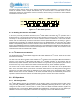
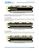
8.8.4 SPI Normal Read
Figure 33 shows the case of a Normal Read operation selected in the OPER field. The operation is
initiated when the I
2
C/SPI Master pulls one of the four nCE signals low. At that point the I
2
C/SPI Master
begins driving the clock onto SCK and the address is transferred from the master to the slave just as it is in
a write operation, but in this case the RW bit is a 0 indicating a read. After the transfer of the last address
bit (bit 0), the I
2
C/SPI Master stops driving the MOSI line and begins loading the FIFO with the data on the
MISO line. The transfer continues until the I
2
C/SPI Master brings the nCE line high.
W 6 1
MOSI
SCK
0 7 6 1 0
Offset Address
nCE
X
Data Byte N
7 6 1 0
Data Byte N+1
X
MISO
5 4 3 2 5 4 3 2 5 4 3 2