
User Manual


Apollo3 Blue Datasheet
DS-A3-0p9p1 Page 268 of 909 2019 Ambiq Micro, Inc.
All rights reserved.
- For multiple commands using DMA, the DMAEN must be reset after the command is done and before
the DMA registers are set for the next transaction.
- It is possible for the CQ to write the REG_IOM_CQADDR register during the CQ operation. The new
address will take effect on the next fetch and allows the CQ to be relocated or looped.
- When starting the CQ operation, 1 doublet will be fetched regardless of the state of the pause status
and bits. If any pause is active, it will take effect after the first fetch. For this reason, it is generally
advisable to have a dummy register write as the first CQ doublet.
- CQ write operations to SW flags used in combination with pause events 15:8 must first disable the
pause enable, perform the SW flag write, then re-enable the pause enable register. SW flags 7:0 can
be written without this restriction and will cause a pause immediately if activated.
8.3 Programmer’s Reference
An example register sequence to initiate an operation is shown below (note this does not show the data
portion of the operation, only the command):
SPI SAMPLE OPERATION:
// Enable clock for 24MHz SPI operation
AM_REG(IOM,CLKFG) =( 0 << AM_REG_IOM_CLKCFG_LOWPER_S) |
( 0 << AM_REG_IOM_CLKCFG_TOTPER_S) |
( 0 << AM_REG_IOM_CLKCFG_DIVEN_S ) |
( 1 << AM_REG_IOM_CLKCFG_DIV3_S ) |
( 1 << AM_REG_IOM_CLKCFG_FSEL_S ) |
( 1 << AM_REG_IOM_CLKCFG_IOCLKEN_S ) ;
// Setup the SPI configuration register.MSB first, no flow control, not full duplex, mode 0
AM_REG(IOM, SPICFG) = ((0 << AM_REG_IOM_MSPICFG_MSPIRST_S) & AM_REG_IOM_MSPICFG_MSPIRST_M)|
((0 << AM_REG_IOM_MSPICFG_DOUTDLY_S) & AM_REG_IOM_MSPICFG_DOUTDLY_M)|
((0 << AM_REG_IOM_MSPICFG_DINDLY_S) & AM_REG_IOM_MSPICFG_DINDLY_M) |
((0 << AM_REG_IOM_MSPICFG_SPILSB_S) & AM_REG_IOM_MSPICFG_SPILSB_M) |
((0 << AM_REG_IOM_MSPICFG_RDFCPOL_S) & AM_REG_IOM_MSPICFG_RDFCPOL_M)|
((0 << AM_REG_IOM_MSPICFG_WTFCPOL_S) & AM_REG_IOM_MSPICFG_WTFCPOL_M)|
((0 << AM_REG_IOM_MSPICFG_WTFCIRQ_S) & AM_REG_IOM_MSPICFG_WTFCIRQ_M)|
((0 << AM_REG_IOM_MSPICFG_MOSIINV_S) & AM_REG_IOM_MSPICFG_MOSIINV_M)|
((0 << AM_REG_IOM_MSPICFG_RDFC_S) & AM_REG_IOM_MSPICFG_RDFC_M)|
((0 << AM_REG_IOM_MSPICFG_WTFC_S) & AM_REG_IOM_MSPICFG_WTFC_M) |
((0 << AM_REG_IOM_MSPICFG_FULLDUP_S) & AM_REG_IOM_MSPICFG_FULLDUP_M)|
((0 << AM_REG_IOM_MSPICFG_SPHA_S) & AM_REG_IOM_MSPICFG_SPHA_M)|
((0 << AM_REG_IOM_MSPICFG_SPOL_S) & AM_REG_IOM_MSPICFG_SPOL_M);
// Send a read command (2) of size 0x20 using 1 byte offset of 0x32 to device on CEN
AM_REG(IOM, CMD) = (( 2 << AM_REG_IOM_CMD_CMD_S) & AM_REG_IOM_CMD_CMD_M) | // READ COMMAND
(( 0 << AM_REG_IOM_CMD_CMDSEL_S) & AM_REG_IOM_CMD_CMDSEL_M)|
(( 0x20 << AM_REG_IOM_CMD_TSIZE_S) & AM_REG_IOM_CMD_TSIZE_M) |
(( 0 << AM_REG_IOM_CMD_CONT_S) & AM_REG_IOM_CMD_CONT_S) |
(( 1 << AM_REG_IOM_CMD_OFFSETCNT_S) & AM_REG_IOM_CMD_OFFSETCNT_M) |
(( 0x32 << AM_REG_IOM_CMD_OFFSETLO_S) & AM_REG_IOM_CMD_OFFSETLO_M);
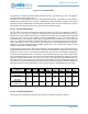
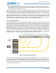
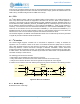
8.4 Interface Clock Generation
The I
2
C/SPI Master can generate a wide range of I/O interface clocks, as shown in Figure 22. The source
clock is a scaled version of the HFRC 48 MHz clock, selected by REG_IOMSTRn_CLKCFG_FSEL. A
divide-by-3 circuit may be selected by REG_IOMSTRn_CLKCFG_DIV3, which is particularly important in
creating a useful SPI frequency of 16 MHz. The output of the divide-by-3 circuit may then be divided by an
8-bit value, REG_IOMSTRn_CLKCFG_TOTPER + 1, to produce the interface clock. This structure allows
very precise specification of the interface frequency, and produces a minimum available interface