
User Manual


Apollo3 Blue Datasheet
DS-A3-0p9p1 Page 267 of 909 2019 Ambiq Micro, Inc.
All rights reserved.
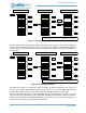
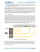
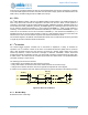
Figure 21. CQ Pause Bit Fetching
The first 8 pause sources (bits 7:0) are register bits which are directly writable via the MCU or
through the CQ. These first 8 locations are called SW Flags. Because the CQ does not support a
read-modify-write operation, special facilities are available to set, reset or toggle the SW Flags.
This is accessed through the REG_IOM_CQSETCLEAR register. The 3 fields in this register
allow a per bit set, reset or toggle of the SW Flag bits.
The next 7 pause sources (bits 14:8) use the SW Flags along with an external signal to set the
pause event. The external signals are from the GPIO module, the MSPI module, or other IOM
modules. On some cases, such as the MSPI interface, 4 of the SW Flags are used and combined
with 2 similar signals from the MSPI module to facilitate a ping pong method of sharing 2 buffers
and preventing overruns without MCU intervention. The logic and connections for each of the
The last pause source (bit 15) is use for index pausing. If this pause bit is enabled, the CQ will
pause when the value of the REG_IOM_CURIDX matches the REG_IOM_ENDIDX. This is
useful for software to be able to update the CQ buffer without causing a race condition between
the CQ data buffer writes and the CQ fetches.
8.2.6.1 CQ programming notes
- Additional restrictions when using the CQ function is that the DMA must be disabled prior to writing the
REG_IOM_CQADDR register, either from the MCU or from the CQ itself.
7 6 5 4 3 2 1 0
7 6 5 4 3 2 1 015 14 13 12 11 10 9 8
REG_IOM_CQPAUSEEN
REG_IOM_CQFLAGS
MSPI 0
MSPI 1
MSPI 0
MSPI 1
GPIO
IOM
BLE
CURIDX
ENDIDX
CURIDX >=
ENDIDX?
OR
PAUSE CQ
IOM CQFLAG OUT
IOM2MSPI_1
IOM2MSPI_0