
User Manual


Apollo3 Blue Datasheet
DS-A3-0p9p1 Page 265 of 909 2019 Ambiq Micro, Inc.
All rights reserved.
- REG_IOM_DMATARGADDR – The source or destination address of the DMA data. Sources can be
either SRAM or FLASH. Destination address can only be SRAM. This is the memory mapped address
of the DMA data as accessed by the MCU.
After the module setup is complete, the command register is written. This will start the IO transfer. The
REG_IOM_CMD register contains the command itself, along with other fields used in the command, such
as channel number, offset counts and transfer size. The IOM supports 2 main commands, read and write.
A read command will write user selectable number of offset bytes (0 to 3), and then read
REG_IOM_CMD.TSIZE bytes, storing the data into the read FIFO. A write command will write the user
selectable number of offset bytes (0 to 3), followed by a write of REG_IOM_CMD.TSIZE bytes sourced
from the write FIFO. Transfer sizes can be 0-255 for I2C and 0-4095 for SPI operations. The number of
offset bytes for each command is specified in the REG_IOM_CMD.OFFSETCNT field.
8.2.6 Command Queue
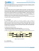
The IOM module can also fetch register write data from SRAM or FLASH, and update the registers as if the
write was performed via the MCU. Register data is stored as a doublet of 2 words. The first word is the
module register address offset, word aligned. The second word is the write data value. Once enabled, the
command queue (CQ) will fetch the address and perform a write to the register If no command is started by
the register write, the next doublet will be fetched by the CQ. If a command is started (write to
REG_IOM_CMD register is done), the CQ processing will wait until the transaction is complete before
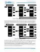
fetching the next register write doublet This is shown in the diagram below. No prefetching is done via the
CQ, and the register write operations are performed in series with the transactions. This allows a
predictable path for execution of commands. DMA enabled commands should be used during CQ
operation, as there is no support to perform a direct mode read operation via the CQ.
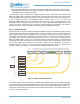
Figure 19. Register Write Data Fetches
The CQ starting fetch address is specified in the REG_IOM_CQADDR register. The CQ operation will start
to fetch when the REG_IOM_CQCFG.CQEN field is set. This field should only be set when the IOM is idle
and the FIFOs are empty. Once enabled, the CQ will continue to fetch sequentially until it encounters a
pause event. A pause event can be caused by a CQ register write operation, or from external signals. This
is shown in the sequence below.
ADDRESS1
WRITEDATA1
ADDRESS2
WRITEDATA2
ADDRESS3
WRITEDATA3
ADDRESS4
WRITEDATA4
CQBUFFER
ADDRESS10
WRITEDATA10
CQFETCHANDWRITE1
(SETUP)
CQFETCHANDWRITE2
(SETUP)
CQFETCHANDWRITE3
(CMDWR)
IOMCMDEXECUTION
CQFETCHANDWRITE4
(SETUP)
CQFETCHAN DWRITE10
(CQENOFF/DISABLE)
TIME