
User Manual


Apollo3 Blue Datasheet
DS-A3-0p9p1 Page 239 of 909 2019 Ambiq Micro, Inc.
All rights reserved.
7.10.2.13FLASH Register
Configuration for XIP/DMA support of SPI flash modules.
OFFSET: 0x0000010C
INSTANCE 0 ADDRESS: 0x5001410C
When any SPI flash is configured, this register must be properly programmed before XIP or AUTO DMA
operations commence.
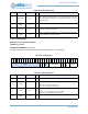
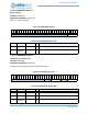
Table 350: PADOUTEN Register
3
1
3
0
2
9
2
8
2
7
2
6
2
5
2
4
2
3
2
2
2
1
2
0
1
9
1
8
1
7
1
6
1
5
1
4
1
3
1
2
1
1
1
0
0
9
0
8
0
7
0
6
0
5
0
4
0
3
0
2
0
1
0
0
RSVD OUTEN
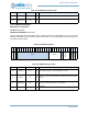
Table 351: PADOUTEN Register Bits
Bit Name Reset RW Description
31:9 RSVD 0x0 RO
RESERVED
8:0 OUTEN 0x0 RW
Output pad enable configuration. Indicates which pads should be driven.
Bits [3:0] are Quad0 data, [7:4] are Quad1 data, and [8] is clock.
QUAD0 = 0x10F - Quad0 (4 data + 1 clock)
QUAD1 = 0x1F0 - Quad1 (4 data + 1 clock)
OCTAL = 0x1FF - Octal (8 data + 1 clock)
SERIAL0 = 0x103 - Serial (2 data + 1 clock)
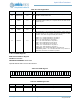
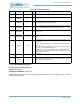
Table 352: FLASH Register
3
1
3
0
2
9
2
8
2
7
2
6
2
5
2
4
2
3
2
2
2
1
2
0
1
9
1
8
1
7
1
6
1
5
1
4
1
3
1
2
1
1
1
0
0
9
0
8
0
7
0
6
0
5
0
4
0
3
0
2
0
1
0
0
READINSTR WRITEINSTR
RSVD
XIPMIXED
XIPSENDI
XIPSENDA
XIPENTURN
XIPBIGENDIAN
XIPACK
RSVD
XIPEN
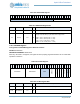
Table 353: FLASH Register Bits
Bit Name Reset RW Description
31:24 READINSTR 0xb RW
Read command sent to flash for DMA/XIP operations
23:16 WRITEINSTR 0x6 RW
Write command sent for DMA operations