
User Manual


Apollo3 Blue Datasheet
DS-A3-0p9p1 Page 238 of 909 2019 Ambiq Micro, Inc.
All rights reserved.
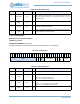
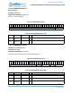
Configuration bits for the MSPI pads. Allows pads associated with the upper quad to be mapped to
corresponding bits on the lower quad. Use of Quad0 pins is recommended for optimal timing.
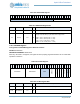
7.10.2.12PADOUTEN Register
MSPI Output Enable Pad Configuration
OFFSET: 0x00000108
INSTANCE 0 ADDRESS: 0x50014108
Enable bits for the MSPI output pads. Each active MSPI line should be set to 1 in the OUTEN field below.
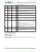
Table 348: PADCFG Register
3
1
3
0
2
9
2
8
2
7
2
6
2
5
2
4
2
3
2
2
2
1
2
0
1
9
1
8
1
7
1
6
1
5
1
4
1
3
1
2
1
1
1
0
0
9
0
8
0
7
0
6
0
5
0
4
0
3
0
2
0
1
0
0
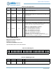
RSVD
REVCS
IN3
IN2
IN1
IN0 RSVD
OUT7
OUT6
OUT5
OUT4
OUT3
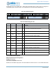
Table 349: PADCFG Register Bits
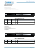
Bit Name Reset RW Description
31:22 RSVD 0x0 RO
RESERVED
21 REVCS 0x0 RW
Reverse CS connections. Allows CS1 to be associated with lower data
lanes and CS0 to be associated with upper data lines
20 IN3 0x0 RW
Data Input pad 3 pin muxing: 0=pad[3] 1=pad[7]
19 IN2 0x0 RW
Data Input pad 2 pin muxing: 0=pad[2] 1=pad[6]
18 IN1 0x0 RW
Data Input pad 1 pin muxing: 0=pad[1] 1=pad[5]
17:16 IN0 0x0 RW
Data Input pad 0 pin muxing: 0=pad[0] 1=pad[4] 2=pad[1] 3=pad[5]
15:5 RSVD 0x0 RO
RESERVED
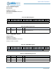
4OUT7 0x0RW
Output pad 7 configuration. 0=data[7] 1=data[3]
3OUT6 0x0RW
Output pad 6 configuration. 0=data[6] 1=data[2]
2OUT5 0x0RW
Output pad 5 configuration. 0=data[5] 1=data[1]
1OUT4 0x0RW
Output pad 4 configuration. 0=data[4] 1=data[0]
0OUT3 0x0RW
Output pad 3 configuration. 0=data[3] 1=CLK