
User Manual


Apollo3 Blue Datasheet
DS-A3-0p9p1 Page 237 of 909 2019 Ambiq Micro, Inc.
All rights reserved.
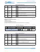
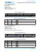
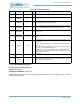
7.10.2.11PADCFG Register
MSPI Output Pad Configuration
OFFSET: 0x00000104
INSTANCE 0 ADDRESS: 0x50014104
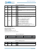
13:8 CLKDIV 0x2 RW
Clock Divider. Allows dividing 48 MHz base clock by integer multiples. Enu-
merations are provided for common frequency, but any integer divide from
48 MHz is allowed. Odd divide ratios will result in a 33/66 percent duty cycle
with a long low clock pulse (to allow longer round-trip for read data).
CLK24 = 0x2 - 24 MHz MSPI clock
CLK12 = 0x4 - 12 MHz MSPI clock
CLK6 = 0x8 - 6 MHz MSPI clock
CLK3 = 0x10 - 3 MHz MSPI clock
CLK1_5 = 0x20 - 1.5 MHz MSPI clock
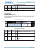
7 RSVD 0x0 RO
RESERVED
6:4 IOMSEL 0x0 RW
Selects which IOM is selected for CQ handshake status.
IOM0 = 0x0 - ERROR: desc VALUE MISSING
IOM1 = 0x1 - ERROR: desc VALUE MISSING
IOM2 = 0x2 - ERROR: desc VALUE MISSING
IOM3 = 0x3 - ERROR: desc VALUE MISSING
IOM4 = 0x4 - ERROR: desc VALUE MISSING
IOM5 = 0x5 - ERROR: desc VALUE MISSING
DISABLED = 0x7 - No IOM selected. Signals always zero.
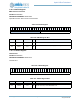
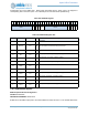
3 TXNEG 0x0 RW
Launches TX data a half clock cycle (~10ns) early. This should normally be
programmed to zero (NORMAL).
NORMAL = 0x0 - TX launched from posedge internal clock
NEGEDGE = 0x1 - TX data launched from negedge of internal clock
2 RXNEG 0x0 RW
Adjusts the RX capture phase to the negedge of the 48MHz internal clock
(~10ns early). For normal operation, it is expected that RXNEG will be set
to 0.
NORMAL = 0x0 - RX data sampled on posedge of internal clock
NEGEDGE = 0x1 - RX data sampled on negedge of internal clock
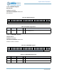
1RXCAP 0x0RW
Controls RX data capture phase. A setting of 0 (NORMAL) captures read
data at the normal capture point relative to the internal clock launch point.
However, to accomodate chip/pad/board delays, a setting of RXCAP of 1 is
expected to be used to align the capture point with the return data window.
This bit is used in conjunction with RXNEG to provide 4 unique capture
points, all about 10ns apart.
NORMAL = 0x0 - RX Capture phase aligns with CPHA setting
DELAY = 0x1 - RX Capture phase is delayed from CPHA setting by one
clock edge
0 APBCLK 0x0 RW
Enable continuous APB clock. For power-efficient operation, APBCLK
should be set to 0.
DIS = 0x0 - Disable continuous clock.
EN = 0x1 - Enable continuous clock.
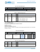
Table 347: MSPICFG Register Bits
Bit Name Reset RW Description