
User Manual


Apollo3 Blue Datasheet
DS-A3-0p9p1 Page 232 of 909 2019 Ambiq Micro, Inc.
All rights reserved.
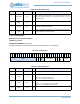
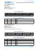
7.10.2.3 ADDR Register
MSPI Transfer Address Register
OFFSET: 0x00000008
INSTANCE 0 ADDRESS: 0x50014008
Optional Address field to send for PIO transfers
13:8 TURNAROUND 0x0 RW
Number of turnaound cycles (for TX->RX transitions). Qualified by
ENTURN or XIPENTURN bit field.
7 SEPIO 0x0 RW
Separate IO configuration. This bit should be set when the target device
has separate MOSI and MISO pins. Respective IN/OUT bits below should
be set to map pins.
6ISIZE 0x0RW
Instruction Size
5:4 ASIZE 0x0 RW
Address Size. Address bytes to send from ADDR register
3:0 DEVCFG 0x1 RW
Flash configuration for XIP and AUTO DMA operations. Controls value for
SER (Slave Enable) for XIP operations and address generation for DMA/
XIP modes. Also used to configure SPIFRF (frame format).
SERIAL0 = 0x1 - Single bit SPI flash on chip select 0
SERIAL1 = 0x2 - Single bit SPI flash on chip select 1
DUAL0 = 0x5 - Dual SPI flash on chip select 0
DUAL1 = 0x6 - Dual bit SPI flash on chip select 1
QUAD0 = 0x9 - Quad SPI flash on chip select 0
QUAD1 = 0xA - Quad SPI flash on chip select 1
OCTAL0 = 0xD - Octal SPI flash on chip select 0
OCTAL1 = 0xE - Octal SPI flash on chip select 1
QUADPAIRED = 0xF - Dual Quad SPI flash on chip selects 0/1.
QUADPAIRED_SERIAL = 0x3 - Dual Quad SPI flash on chip selects 0/1,
but transmit in serial mode for initialization operations
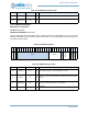
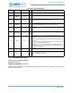
Table 332: ADDR Register
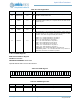
3
1
3
0
2
9
2
8
2
7
2
6
2
5
2
4
2
3
2
2
2
1
2
0
1
9
1
8
1
7
1
6
1
5
1
4
1
3
1
2
1
1
1
0
0
9
0
8
0
7
0
6
0
5
0
4
0
3
0
2
0
1
0
0
ADDR
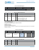
Table 333: ADDR Register Bits
Bit Name Reset RW Description
31:0 ADDR 0x0 RW
Optional Address field to send (after optional instruction field) - qualified by
ASIZE in CMD register. NOTE: This register is aliased to DMADEVADDR.
Table 331: CFG Register Bits
Bit Name Reset RW Description