
User Manual


Apollo3 Blue Datasheet
DS-A3-0p9p1 Page 231 of 909 2019 Ambiq Micro, Inc.
All rights reserved.
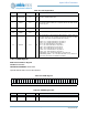
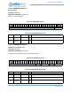
7.10.2.2 CFG Register
MSPI Transfer Configuration Register
OFFSET: 0x00000004
INSTANCE 0 ADDRESS: 0x50014004
Command formatting for PIO based transactions (initiated by writes to CTRL register)
3QUADCMD 0x0RW
Flag indicating that the operation is a command that should be replicated to
both devices in paired QUAD mode. This is typically only used when read-
ing/writing configuration registers in paired flash devices (do not set for
memory transfers).
2 BUSY 0x0 RO
Command status: 1 indicates controller is busy (command in progress)
1STATUS 0x0RO
Command status: 1 indicates command has completed. Cleared by writing
1 to this bit or starting a new transfer.
0START 0x0RW
Write to 1 to initiate a PIO transaction on the bus (typically the entire register
should be written at once with this bit set).
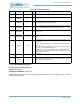
Table 330: CFG Register
3
1
3
0
2
9
2
8
2
7
2
6
2
5
2
4
2
3
2
2
2
1
2
0
1
9
1
8
1
7
1
6
1
5
1
4
1
3
1
2
1
1
1
0
0
9
0
8
0
7
0
6
0
5
0
4
0
3
0
2
0
1
0
0
RSVD
CPOL
CPHA
RSVD
TURNAROUND
SEPIO
ISIZE
ASIZE
DEVCFG
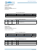
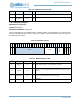
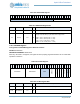
Table 331: CFG Register Bits
Bit Name Reset RW Description
31:18 RSVD 0x0 RO
RESERVED
17 CPOL 0x0 RW
Serial clock polarity.
LOW = 0x0 - Clock inactive state is low.
HIGH = 0x1 - Clock inactive state is high.
16 CPHA 0x0 RW
Serial clock phase.
MIDDLE = 0x0 - Clock toggles in middle of data bit.
START = 0x1 - Clock toggles at start of data bit.
15:14 RSVD 0x0 RO
RESERVED
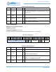
Table 329: CTRL Register Bits
Bit Name Reset RW Description