
User Manual

Apollo3 Blue Datasheet
DS-A3-0p9p1 Page 230 of 909 2019 Ambiq Micro, Inc.
All rights reserved.
7.10.2 MSPI Registers
7.10.2.1 CTRL Register
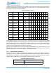
MSPI PIO Transfer Control/Status Register
OFFSET: 0x00000000
INSTANCE 0 ADDRESS: 0x50014000
This register is used to enable individual PIO based transactions to a device on the bus. The CFG register
must be programmed properly for the transfer, and the ADDR and INSTR registers should be programmed
if the SENDI and SENDA fields are enabled.
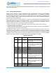
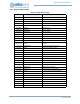
Table 328: CTRL Register
3
1
3
0
2
9
2
8
2
7
2
6
2
5
2
4
2
3
2
2
2
1
2
0
1
9
1
8
1
7
1
6
1
5
1
4
1
3
1
2
1
1
1
0
0
9
0
8
0
7
0
6
0
5
0
4
0
3
0
2
0
1
0
0
XFERBYTES
RSVD
PIOSCRAMBLE
TXRX
SENDI
SENDA
ENTURN
BIGENDIAN
RSVD
QUADCMD
BUSY
STATUS
START
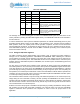
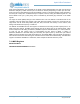
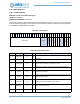
Table 329: CTRL Register Bits
Bit Name Reset RW Description
31:16 XFERBYTES 0x0 RW
Number of bytes to transmit or receive (based on TXRX bit)
15:12 RSVD 0x0 RO
RESERVED
11 PIOSCRAMBLE 0x0 RW
Enables data scrambling for PIO opertions. This should only be used for
data operations and never for commands to a device.
10 TXRX 0x0 RW
1 Indicates a TX operation, 0 indicates an RX operation of XFERBYTES
9 SENDI 0x0 RW
Indicates whether an instruction phase should be sent (see INSTR field and
ISIZE field in CFG register)
8 SENDA 0x0 RW
Indicates whether an address phase should be sent (see ADDR register and
ASIZE field in CFG register)
7 ENTURN 0x0 RW
Indicates whether TX->RX turnaround cycles should be enabled for this
operation (see TURNAROUND field in CFG register).
6 BIGENDIAN 0x0 RW
1 indicates data in FIFO is in big endian format (MSB first); 0 indicates little
endian data (default, LSB first).
5:4 RSVD 0x0 RO
RESERVED