
User Manual

Apollo3 Blue Datasheet
DS-A3-0p9p1 Page 228 of 909 2019 Ambiq Micro, Inc.
All rights reserved.
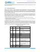
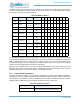
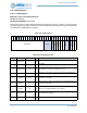
Note that bit transmission from the MSPI to the target is fairly straightforward since both the SCLK and
MOSI are delayed by similar amounts (two red arrows on the left). Depending on which pins are used,
there may be some skew between the SCLK and MOSI, however, it should be relatively small compared to
the half-cycle of setup time. If additional setup is required, however, setting the TXNEG register to 1 will
launch MOSI a half cycle (~10ns) early, which is indicated by the dotted gray waveform on the MOSI
signals.
The target to master (MISO) timings on SPI interfaces are a bit more difficult to handle because of the
cumulative round trip delay that consists of the clock delay from master to target, the access time at the
target itself, and the return delay MISO path (first, third, and fourth red arrows). For this reason, read
timings often dictate the frequency of a SPI bus.
The RXCAP and RXNEG bits are used together to determine the incoming RX data capture point. In an
ideal world (zero delays), the MSPI would capture data at the rising edge of the internal SCLK, which
would correspond to the setting of RXCAP=0, RXNEG=0 (the first vertical blue bar). It is useful, however,
to push out the RX capture point to accommodate the late arrival of MISO. A setting of
RXCAP=1,RXNEG=0 is the ideal setting and will delay the capture point by about 20ns (one internal
48MHz clock) as indicated in the third vertical blue line. At a 24MHz MSPI clock this should correspond to
about the time the device starts driving the next data and thus should be the ideal setting. The MSPI also
supports an RXCAP=1/RXNEG=1 combination, which samples in between these two points.
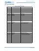
7.10 MSPI Registers
Multibit SPI Master
INSTANCE 0 BASE ADDRESS:0x50014000