
User Manual

Apollo3 Blue Datasheet
DS-A3-0p9p1 Page 227 of 909 2019 Ambiq Micro, Inc.
All rights reserved.
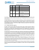
Since the data lines within a quad are balanced with respect to each other, it is recommended that
customers do not use the internal muxing features unless pin requirements disallow the use of a
contiguous quad.
7.9.2 MSPI Pin Timing Board/Package Considerations
The MSPI pins in the chip pin muxing are grouped by the two sets of quad pairs. The lower MSPI quad
should be used whenever possible since these pads are closer to the MSPI logic and have less delay than
the upper quad. When running in octal mode, the timings through the upper pins will dictate the speed of
the interface.
The MSPI logic contains controls to adjust I/O timings to accommodate differences in board or device
timings through the RXCAP, RXNEG, and TXNEG bits in the MSPICFG register. The discussion below
assumes SPI mode 0 (CPHA=0, CPOL=0) and that in dual/quad/octal modes that MOSI refers to all pins in
transmission mode and MISO refers to all pins when in receive mode.
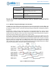
If there were no delays in the chip/board/device, then ideally, data is launched on the negedge of the clock
and captured on the posedge of the clock at both the master (MSPI) and target (flash) device. However the
presence of delays in the system complicates timing and the timing diagram shown in Figure 13 indicates
how these delays are accommodated in the MSPI interface design. The CLK (int) refers to the internal
48MHz clock used by the MSPI, and the SCLK/MOSI (int) are the internal chip timings for the outgoing
clock and MOSI lines. Likewise, the @ Dev signals indicate the timing at the target device's pins. (Delays
shown are just representative and may not reflect actual device timings.)
Figure 13. MSPI Interface Diagram
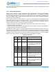
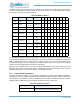
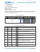
IN3,IN2,IN1,IN0
Allows muxing of individual bit inputs from the upper
quad (MSPI data bits 7:4) into the lower quad. Typically
the OUT7-4 bits would be set to match.
OUT7,OUT6,OUT5,OUT4
Allows muxing of individual bit outputs from the lower
quad to the upper quad. Typically the IN3-0 bits would
be set to match.
OUT3 Allows MSPI pin [3] to be used as the clock output.
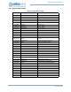
Table 326: PADCFG Description
Bitfield Description