
User Manual

Apollo3 Blue Datasheet
DS-A3-0p9p1 Page 226 of 909 2019 Ambiq Micro, Inc.
All rights reserved.
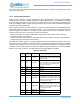
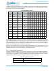
The MSPI supports the following external connections. The columns to the right indicate which bits are
used in each configuration (S=serial, D=dual, Q=quad, QP=quad-pair, O=octal with CE#). Within the table,
O=output pin, I=input pin, and X=bidirectional.
The PADOUTEN register should be programmed to enable the proper pins for the selected mode. While
the MSPI will automatically drive and sample data from the proper data lines, the MSPI also contains the
ability to map bit lanes from the lower quad to the upper quad in case the system-level design cannot
accommodate mapping the four contiguous pins within the lower quad. This is done via the PADCFG
register, which has separate input and output muxing options.
Typically, most serial SPI devices use a separate MOSI and MISO when operating in serial mode. The
SEPIO bit should be set when software needs to read data from devices in serial mode, since it redirects
the MISO input from pin 1 down to input data pin 0 of the MSPI's RX logic.
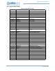
7.9.1 Internal Pin Muxing Options
The MSPI also has the ability to swap some pin functionality to provide some additional flexibility in
selecting pins used by the MSPI. Table 325 shows the MSPI pin mapping through the GPIO module, which
has fixed pads for each MSPI pin, however, the MSPI can also perform a minimal second layer of function
swapping within the MSPI pins using the PADCFG register as shown in Table 326.
Table 325: MSPI Pin Muxing
Pin Name Direction GPIO Description S0 S1 D0 D1 Q0 Q1 QP O0 O1
ce0 Output
1,7,10,15,19,
28
MSPI CE0 O O O O O
ce1 Output
12,32,36,41,
43,46
MSPI CE1 O O O O O
mspi8 Output 24 MSPI CLK O O O O O O O O O
mspi7 Input/Output 3
MSPI Data
Bit7
XXXX
mspi6 Input/Output 2
MSPI Data
Bit6
XXXX
mspi5 Input/Output 1
MSPI Data
Bit5
IXXXXX
mspi4 Input/Output 0
MSPI Data
Bit4
OX XXXX
mspi3 Input/Output 23
MSPI Data
Bit3
XXXX
mspi2 Input/Output 4
MSPI Data
Bit2
XXXX
mspi1 Input/Output 26
MSPI Data
Bit1
IXXXXX
mspi0 Input/Output 22
MSPI Data
Bit0
OX XXXX
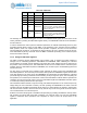
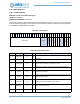
Table 326: PADCFG Description
Bitfield Description
REVCS
Swaps chip enable outputs, allowing pins mapped to
CS1 to be associated with the lower quad of data pins.