
User Manual

Apollo3 Blue Datasheet
DS-A3-0p9p1 Page 221 of 909 2019 Ambiq Micro, Inc.
All rights reserved.
7.5.3 Micron XIP Support
Micron flash devices support an XIP mode that does not require the instruction byte to be transmitted,
which minimizes the access time to the device. In order to transition in and out of this mode, the MSPI
controller must issue an acknowledgment of XIP mode during the first turnaround cycle for each XIP
access. When transitioning into and out of XIP mode, software must set the XIPACK field of the MSPI's
FLASH register appropriately.
Under normal operation, the XIPACK should be set to NOACK (0x0), indicating that no acknowledgment
should be sent. To transition into XIP mode, software should perform the following actions:
1. Activate XIP in the Micron device by writing the Volatile Configuration register
2. Set the XIPACK bit field in the MSPI FLASH register to ACK (0x2)
3. Perform a memory read from the Micron device (instruction must be sent). This access will allow
the MSPI controller to acknowledge switching into the XIP mode
4. Set the XIPSENDI bit field in the MSPI FLASH register to 0 to indicate that the instruction byte no
longer needs to be sent.
The MSPI will now transmit just the address to the Micron device and drive a 0 onto the data lines on the
first turnaround cycle to remain in XIP mode. It is important that software ONLY perform read operations to
the flash device until XIP mode has been exited.
To terminate XIP mode, software should perform the following sequence:
1. Set the XIPACK bit field in the MSPI FLASH register to TERMINATE (0x3)
2. Issue a memory read to the Micron device. This will allow the MSPI controller to signal termination
of XIP mode by driving the data lines high during the first turnaround cycle.
3. Set the XIPACK bit field to NOACK (0x0) and the XIPSENDI bit field to 1
After this sequence has completed, software can erase, program, or send any other instructions to the
Micron flash again.
7.6 Command Queueing (CQ)
The MSPI's command queuing (CQ) interface is similar to command queuing implementation in the IOM
and BLE modules. To utilize the command queue, software basically constructs a series of register
operations that would be issued to the MSPI device, but instead places them in an array in system SRAM
(or internal flash). The start of this buffer is then written to the CQADDR register and the commands can
issued by enabling the CQEN bit in the CQCFG register. The CQ logic then reads the address/data pairs
via DMA operations and will continue executing them until the end of the command queue, which is
denoted as a write to the STOP bit in the CQPAUSE register. As the CQ logic issues register operations, it
will automatically pause fetching new operations while the transfer module is busy or can be paused to
wait for external events based on the status of the CQPAUSE and CQFLAGS registers.
The primary limitation of CQ operations is that all addresses must reside within the MSPI module since the
operations are executed internally by the MSPI module (i.e. it cannot write register in other modules, etc).
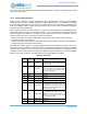
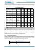
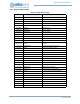
7.6.1 Command Queue Data Format
As the command queue resides in system memory, the general format is pairs of words that form the
register address to write as well as the data to write. Assuming the CQ base address is 0x10000, system
SRAM might look like the following table: