
User Manual
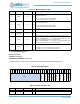


Apollo3 Blue Datasheet
DS-A3-0p9p1 Page 220 of 909 2019 Ambiq Micro, Inc.
All rights reserved.
7.5 Execute in Place (XIP) Operations
The XIP mode of operation allows devices on the MSPI interface to be
mapped into the flash cache's address space and appear as an
extension to the internal flash array(s). Once enabled by the XIPEN bit
in the FLASH register, the flash/cache module will decode the address
region and forward operations to the MSPI interface for completion. XIP
mode uses the same configuration information as DMA mode and will
automatically execute a cache line read fetch from the attached device
and return it to the cache controller.
XIP and DMA/PIO operations can all be interleaved since the MSPI
controller will allow the current operation to complete before performing
the XIP operation. Generally DMA read operations can safely be
interleaved with XIP, however, XIP mode may have to be disabled
during flash programming operations since the flash array within the
device may not be available during program or erase operations and thus would return invalid data.
7.5.1 XIPMM Operation
For Apollo3 Rev B, the MSPI additionally supports a memory-mapped XIP mode (XIPMM) that enables full
read/write mapping of an MSPI device such as a PSRAM to the CPU's peripheral address map at offset
0x51000000-0x51FFFFFF. This is mapped to offset 0 of the device on the MSPI bus and is not cached
(unlike XIP space) and thus can be used as an extension to system SRAM. The MSPI device can be
accessed by both XIP and XIPMM accesses (the regions overlap), but it is recommended that XIP used for
static data/instructions and that a separate area of the MSPI device is used for read/write operations to
avoid having stale data visible in the cache.
XIPMM seamlessly supports word, halfword, and byte read and write accesses, however, there are a few
restrictions and caveats:
As mentioned above, writes to XIPMM do not flush cached data to the same address.
For scrambled regions, XIPMM can only be written safely by writing words (byte and halfword writes will
corrupt the scrambled data at that location). Byte, halfword, and word reads may all be performed to
scrambled regions.
Read/Write performance to the XIPMM region will be significantly slower than accesses to internal SRAM
since there are multiple cycles of command, addressing, and data transfer overhead. For this reason,
internal SRAM should be used for frequently accessed data and XIPMM should be used for infrequently
used data.
To help minimize the access penalty on XIPMM writes, a 2-entry write FIFO buffers all writes to XIPMM.
These will be immediately accepted on the CPU's bus allowing it to continue execution. However, the CPU
will stall if another write or peripheral read is performed before the previous writes complete.
7.5.2 Optimized XIP Addressing
Some SPI flash devices support an optimized XIP mode that minimizes the number of instruction/address
cycles that must be transmitted in order to reduce overall fetch latency. To activate this mode, software
should program the flash device's registers to enter the device XIP mode, and then update the DEVCFG
field to the specified number of address bytes and then disable the XIPSENDI field in the FLASH register
(assuming that no instruction needs to be sent). To exit the device's XIP mode, software should reconfigure
the MSPI interface in order to send the required XIP exit sequence to the device.