
User Manual


Apollo3 Blue Datasheet
DS-A3-0p9p1 Page 217 of 909 2019 Ambiq Micro, Inc.
All rights reserved.
7.2 Configuration
The MSPI module should be configured to match the transfer characteristics of the external device(s) on
the bus. Generally, the configuration sequence would proceed as follows:
▪ Configure MSPI clock divider (MSPICFG register). The MSPI's reference frequency is 48MHz, so the
resulting clock frequency is 48/CLKDIV value.
▪ Configure MSPI transfer characteristics (CFG register) to initialize the device (usually mode 0, serial
transfers)
▪ Configure MSPI PADOUTEN to enable the desired bits on the MSPI bus (clock plus relevant data bits).
NOTE: Enabling unused data lines will impact the values present on those pads even if the GPIO func-
tion select is not set to MSPI.
▪ Program external flash device to the appropriate mode, enable dual/quad/octal modes
▪ Update CFG register to new settings (in cases of a transfer mode or addressing change)
▪ Write FLASH register to set read/write instructions and transfer characteristics for DMA/XIP operations
(and optionally enable XIP mode).
The MSPI's CFG register contains the controller's settings when communicating with any given device and
it is expected that these values will be static after initial configuration of the external memory devices. The
DEVCFG field specifies both the transfer mode (serial, dual, quad, etc) as well as which chip enable is
used to access the device. The ISIZE and ASIZE fields indicate the number of bytes transmitted for the
instruction and address phases, but individual operations can select whether to transmit these or not. The
TURNAROUND field indicates the number of cycles between the TX of instruction/address and reception
of the first RX byte (the flash device must be programmed to use the same count). Finally, the CPOL and
CPHA fields indicate the settings for the clock polarity and clock phase settings, which are often
referenced in literature as SPI modes 0-3. Most memory devices utilize mode 0 (CPOL=0, CPHA=0).
7.3 PIO Operations
Software can issue general PIO operations to devices on the MSPI bus using the INSTR, ADDR, and
CTRL registers. Software should first write the instruction to be sent to the INSTR register and the address
to be sent to the ADDR register (if required) followed by a write to the CTRL register to start the transfer.
The TXRX bit indicates whether data should flow to or from the device and XFERBYTES indicates the
number of bytes to transfer. SENDI and SENDA can be used to enable or disable the instruction or
address phases and the ENTURN is used to enable the turnaround phase. The transfer will only
commence if the START bit is set. Software may read the BUSY and STATUS fields to check on
transaction status, otherwise the CMDCPL interrupt can be used to indicate completion.
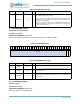
AM_REG(MSPI,INSTR) = instr;
AM_REG(MSPI,CTRL) = AM_REG_MSPI_CTRL_XFERBYTES(bytes) |
AM_REG_MSPI_CTRL_SENDI_M |
AM_REG_MSPI_CTRL_TXRX(1) |
AM_REG_MSPI_CTRL_START_M;
For write (TX) operations, data should be written to the TXFIFO after the transaction has been started.
Software should read TXENTRIES before writing to ensure that space is available in the FIFO before
writing new TX data. For read operations, software should read the RXENTRIES to determine the number
of words available and then read the data from the RXFIFO register.
// Example TX data write loop
for (i = 0; i < count; ) {
temp1=AM_REG(MSPI,TXENTRIES);
for(;(temp1<16) && (i<count);temp1++,i++) {
AM_REG(MSPI,TXFIFO) = data[i];
}
}