
User Manual


Apollo3 Blue Datasheet
DS-A3-0p9p1 Page 216 of 909 2019 Ambiq Micro, Inc.
All rights reserved.
7. MSPI Master Module
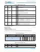
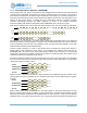
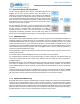
Figure 12. Block Diagram for the MSPI Master Module
7.1 Functional Overview
The Apollo3 MCU includes a Multi-bit SPI (MSPI) module which can be used to connect to external serial
memory devices. It supports operation up to 24 MHz, all four SPI CPOL/CPHA modes, and can transfer in
serial, dual, quad, and octal modes (with a single octal device or a pair of quad devices). The MSPI module
has a unified 16-entry FIFO (32 bits wide) that is used for both transmit and receive data. To ensure that
transactions are not dropped because of system or software latency, the MSPI controller will pause the
clock (and thus the transfer on the bus) if the TX FIFO empties or the RX FIFO fills during an operation. It
will automatically resume once the FIFO condition has cleared.
MSPI transfers generally consist of transmitting a 1 byte instruction, a 1-4 byte address (optional), and 1
byte to 64KB of write or read data (with an optional number of turnaround clock cycles between address
and RX data). Access to flash devices are supported through PIO operations (primarily for configuration
operations), through DMA operations to automatically transfer data blocks to/from the flash, and through
an XIP mode, where instructions/data can be accessed in the external flash memory through an aperture
in the integrated flash cache. The MSPI module also supports data scrambling of external accesses within
an address window having boundaries aligned to 64K address blocks.
Once the external devices are configured, the MSPI supports a simple DMA model, where software can
program the internal (SRAM or flash) address and external device address, transfer direction, and transfer
size. Once enabled, the MSPI DMA interface will move data between the system and external flash and
interrupt when complete. The MSPI also supports a higher-level command queuing (CQ) protocol, where
software can construct a buffer of operations in SRAM (or internal flash memory) and the MSPI will
execute the series of operations autonomously. The MSPI can also power itself down at the end of DMA or
CQ operations.
While the MSPI module can be used as a generic SPI device (with two chip enables), it is primarily
designed to support serial NAND/NOR flash memory and is intended to be used to initialize the external
memory devices and then configured with the parameters matching the flash access characteristics.
Devices can then be accessed through DMA or XIP operations with minimal software overhead.
Bus Interface
CMD Queue
DMA
XiP
REGs
INTs
MSPI Controller
Rx FIFO
1 / 2 / 4 / 8 bit I/O
Tx FIFO