
User Manual


Apollo3 Blue Datasheet
DS-A3-0p9p1 Page 211 of 909 2019 Ambiq Micro, Inc.
All rights reserved.
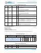
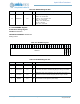
6.3.2.33 BLECFG Register
BLE Core Control
OFFSET: 0x00000304
INSTANCE 0 ADDRESS: 0x5000C304
Provides control of isolation and IO signals between the interface module and the BLE Core.
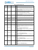
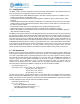
17 RDFC 0x0 RW
Enables flow control of new read transactions based on the SPI_STATUS
signal from the BLE Core.
DIS = 0x0 - Read mode flow control disabled.
EN = 0x1 - Read mode flow control enabled.
16 WTFC 0x0 RW
Enables flow control of new write transactions based on the SPI_STATUS
signal from the BLE Core.
DIS = 0x0 - Write mode flow control disabled.
EN = 0x1 - Write mode flow control enabled.
15:3 RSVD 0x0 R0
Reserved
2 FULLDUP 0x0 RW
Full Duplex mode. Capture read data during writes operations
1 SPHA 0x0 RW
Selects the SPI phase; When 1, will shift the sampling edge by 1/2 clock.
SAMPLE_LEADING_EDGE = 0x0 - Sample on the leading (first) clock
edge, rising or falling dependent on the value of SPOL
SAMPLE_TRAILING_EDGE = 0x1 - Sample on the trailing (second) clock
edge, rising of falling dependent on the value of SPOL
0 SPOL 0x0 RW
This bit selects SPI polarity.
CLK_BASE_0 = 0x0 - The initial value of the clock is 0.
CLK_BASE_1 = 0x1 - The initial value of the clock is 1.
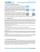
Table 315: BLECFG Register
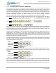
3
1
3
0
2
9
2
8
2
7
2
6
2
5
2
4
2
3
2
2
2
1
2
0
1
9
1
8
1
7
1
6
1
5
1
4
1
3
1
2
1
1
1
0
0
9
0
8
0
7
0
6
0
5
0
4
0
3
0
2
0
1
0
0
RSVD
SPIISOCTL
PWRISOCTL
STAYASLEEP
FRCCLK
MCUFRCSLP
WT4ACTOFF
BLEHREQCTL
DCDCFLGCTL
WAKEUPCTL
BLERSTN
PWRSMEN
Table 316: BLECFG Register Bits
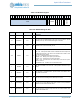
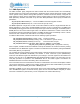
Bit Name Reset RW Description
31:16 RSVD 0x0 RO
RESERVED
Table 314: MSPICFG Register Bits
Bit Name Reset RW Description