
User Manual


Apollo3 Blue Datasheet
DS-A3-0p9p1 Page 204 of 909 2019 Ambiq Micro, Inc.
All rights reserved.
6.3.2.24 CQADDR Register
CQ Target Read Address Register
OFFSET: 0x0000024C
INSTANCE 0 ADDRESS: 0x5000C24C
The SRAM address which will be fetched next execution of the CQ operation. This register is updated as
the CQ operation progresses, and is the live version of the register. The register can also be
6.3.2.25 CQSTAT Register
Command Queue Status Register
OFFSET: 0x00000250
INSTANCE 0 ADDRESS: 0x5000C250
Provides the status of the command queue operation. If the command queue is disabled, these bits will be
cleared. The bits are read only
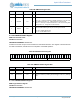
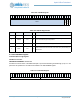
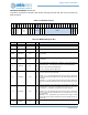
Table 297: CQADDR Register
3
1
3
0
2
9
2
8
2
7
2
6
2
5
2
4
2
3
2
2
2
1
2
0
1
9
1
8
1
7
1
6
1
5
1
4
1
3
1
2
1
1
1
0
0
9
0
8
0
7
0
6
0
5
0
4
0
3
0
2
0
1
0
0
RSRVD2
CQADDR28
RSRVD1 CQADDR
RSRVD0
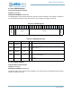
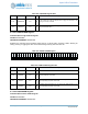
Table 298: CQADDR Register Bits
Bit Name Reset RW Description
31:29 RSRVD2 0x0 RO
Reserved
28 CQADDR28 0x0 RW
Bit 28 of target byte address for source of CQ. Used to denote Flash (0) or
SRAM (1) access
27:20 RSRVD1 0x0 RO
Reserved
19:2 CQADDR 0x0 RW
Bits 19:2 of target byte address for source of CQ. The buffer must be
aligned on a word boundary
1:0 RSRVD0 0x0 RO
Reserved