
User Manual


Apollo3 Blue Datasheet
DS-A3-0p9p1 Page 202 of 909 2019 Ambiq Micro, Inc.
All rights reserved.
The source or destination address internal the SRAM for the DMA data. For write operations, this can
only be SRAM data (ADDR bit 28 = 1); For read operations, this can be either SRAM or FLASH (ADDR bit
28 = 0)
6.3.2.22 DMASTAT Register
DMA Status Register
OFFSET: 0x00000244
INSTANCE 0 ADDRESS: 0x5000C244
Status of the DMA operation currently in progress.
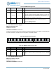
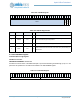
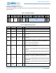
Table 291: DMATARGADDR Register
3
1
3
0
2
9
2
8
2
7
2
6
2
5
2
4
2
3
2
2
2
1
2
0
1
9
1
8
1
7
1
6
1
5
1
4
1
3
1
2
1
1
1
0
0
9
0
8
0
7
0
6
0
5
0
4
0
3
0
2
0
1
0
0
RSVD
TARGADDR28
RSVD TARGADDR
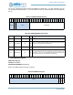
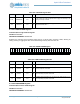
Table 292: DMATARGADDR Register Bits
Bit Name Reset RW Description
31:29 RSVD 0x0 RO
Reserved
28 TARGADDR28 0x0 RW
Bit 28 of the target byte address for source of DMA (either read or write). In
cases of non-word aligned addresses, the DMA logic will take care for
ensuring only the target bytes are read/written.
27:20 RSVD 0x0 RO
Reserved
19:0 TARGADDR 0x0 RW
Bits [19:0] of the target byte address for source of DMA (either read or
write). The address can be any byte alignment, and does not have to be
word aligned. In cases of non-word aligned addresses, the DMA logic will
take care for ensuring only the target bytes are read/written.
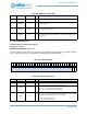
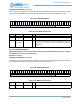
Table 293: DMASTAT Register
3
1
3
0
2
9
2
8
2
7
2
6
2
5
2
4
2
3
2
2
2
1
2
0
1
9
1
8
1
7
1
6
1
5
1
4
1
3
1
2
1
1
1
0
0
9
0
8
0
7
0
6
0
5
0
4
0
3
0
2
0
1
0
0
RSVD
DMAERR
DMACPL
DMATIP