
User Manual


Apollo3 Blue Datasheet
DS-A3-0p9p1 Page 187 of 909 2019 Ambiq Micro, Inc.
All rights reserved.
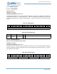
6.3.2.8 CLKCFG Register
I/O Clock Configuration
OFFSET: 0x00000200
INSTANCE 0 ADDRESS: 0x5000C200
Provides clock related controls used internal to the BLEIF module, and enablement of 32KHz clock to the
BLE Core module. The internal clock sourced is selected via the FSEL and can be further divided by 3
using the DIV3 control.
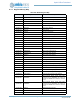
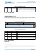
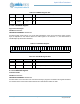
Table 263: FIFOLOC Register
3
1
3
0
2
9
2
8
2
7
2
6
2
5
2
4
2
3
2
2
2
1
2
0
1
9
1
8
1
7
1
6
1
5
1
4
1
3
1
2
1
1
1
0
0
9
0
8
0
7
0
6
0
5
0
4
0
3
0
2
0
1
0
0
RSVD
FIFORPTR
RSVD
FIFOWPTR
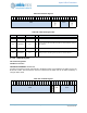
Table 264: FIFOLOC Register Bits
Bit Name Reset RW Description
31:12 RSVD 0x0 RO
Reserved
11:8 FIFORPTR 0x0 RW
Current FIFO read pointer. Used to index into the incoming FIFO (FIFO1),
which is used to store read data returned from external devices during a
read operation.
7:4 RSVD 0x0 RO
Reserved
3:0 FIFOWPTR 0x0 RW
Current FIFO write pointer. Value is the index into the outgoing FIFO
(FIFO0), which is used during write operations to external devices.
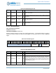
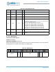
Table 265: CLKCFG Register
3
1
3
0
2
9
2
8
2
7
2
6
2
5
2
4
2
3
2
2
2
1
2
0
1
9
1
8
1
7
1
6
1
5
1
4
1
3
1
2
1
1
1
0
0
9
0
8
0
7
0
6
0
5
0
4
0
3
0
2
0
1
0
0
RSVD
DIV3
CLK32KEN
FSEL RSVD
IOCLKEN