
User Manual


Apollo3 Blue Datasheet
DS-A3-0p9p1 Page 170 of 909 2019 Ambiq Micro, Inc.
All rights reserved.
3.9.3.3 Flash Memory Controller
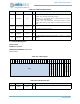
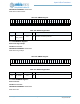
Figure 7. Block diagram for the Flash Memory Controller
3.9.3.3.1 Functional Overview
During normal MCU code execution, the Flash Memory Controller translates requests from the CPU core
(via the Flash cache) to the Flash Memory instance for instruction and data fetches. The Controller is
designed to return data to the cache in single wait-state and can operate up to the maximum operating
frequency of half the CPU core frequency.
The Controller facilitates flash erase and programming operations through the control registers. When
erase or programming operations are active, data cannot be fetched from the Flash memory. This will be
naturally handled by the cache controller fill logic to stall until the program operation is complete and the
Flash device is available. With the cache enabled, this collision should happen very infrequently.
Another function of the Controller is to capture the configuration values which are distributed to the various
on-chip peripherals of the MCU at chip power-up. These are read from the Information Space of the Flash
Memory and captured in registers to be used by the other peripherals. The configuration values are
reloaded each time a full-chip POI cycle occurs.
Note: Programming the same bit cannot be reprogrammed to a ‘0’ before an erase cycle. Doing so may
cause data corruption/retention issues within the word line. Ambiq provides a “modify” function to help with
this.
Note: The number of program cycles performed per word line (512 bytes) should be limited to no more
than 160 between erase cycles. Alternatively, 1 full line program plus 100 additional program cycles to the
AHB Slave
(Info Space)
APB Slave
(Control
Regs)
APB Slave
(Config
Regs)
Config
Registers
Control
Registers
Timing
Control
Flash
Instance
Copy
Engine
Request
Translator
Request
Translator
AHB Slave
(DCode)
Request
Translator
AHB Slave
(ICode)
Request
Translator