
User Manual


Apollo3 Blue Datasheet
DS-A3-0p9p1 Page 162 of 909 2019 Ambiq Micro, Inc.
All rights reserved.
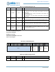
3.9.3.2.2.3CTRL Register
Cache Control
OFFSET: 0x00000008
INSTANCE 0 ADDRESS: 0x40018008
Cache Control
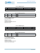
13:12 LPMMODE 0x0 RW
Controls flash low power modes (control of LPM pin).
NEVER = 0x0 - High power mode (LPM not used).
STANDBY = 0x1 - Fast Standby mode. LPM deasserted for read opera-
tions, but asserted while flash IDLE.
ALWAYS = 0x2 - Low Power mode. LPM always asserted for reads.
LPM_RD_WAIT must be programmed to accomodate longer read access
times.
11:8 LPM_RD_WAIT 0x8 RW
Sets flash waitstates when in LPM Mode 2 (RD_WAIT in LPM mode 2 only)
7 RSVD 0x0 RO
This bitfield is reserved for future use.
6:4 SEDELAY 0x7 RW
Sets SE delay (flash address setup). A value of 5 is recommended.
3:0 RD_WAIT 0x3 RW
Sets read waitstates for normal (fast) operation. A value of 1 is recom-
mended.
Table 224: CTRL Register
3
1
3
0
2
9
2
8
2
7
2
6
2
5
2
4
2
3
2
2
2
1
2
0
1
9
1
8
1
7
1
6
1
5
1
4
1
3
1
2
1
1
1
0
0
9
0
8
0
7
0
6
0
5
0
4
0
3
0
2
0
1
0
0
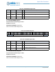
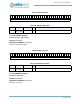
RSVD
FLASH1_SLM_ENABLE
FLASH1_SLM_DISABLE
FLASH1_SLM_STATUS
RSVD
FLASH0_SLM_ENABLE
FLASH0_SLM_DISABLE
FLASH0_SLM_STATUS
RSVD
CACHE_READY
RESET_STAT
INVALIDATE
Table 225: CTRL Register Bits
Bit Name Reset RW Description
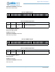
31:11 RSVD 0x0 RO
This bitfield is reserved for future use.
Table 223: FLASHCFG Register Bits
Bit Name Reset RW Description