
User Manual


Apollo3 Blue Datasheet
DS-A3-0p9p1 Page 161 of 909 2019 Ambiq Micro, Inc.
All rights reserved.
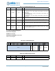
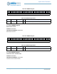
3.9.3.2.2.2FLASHCFG Register
Flash Control Register
OFFSET: 0x00000004
INSTANCE 0 ADDRESS: 0x40018004
Flash Control Register
7:4 CONFIG 0x5 RW
Sets the cache configuration
W1_128B_512E = 0x4 - Direct mapped, 128-bit linesize, 512 entries (4
SRAMs active)
W2_128B_512E = 0x5 - Two-way set associative, 128-bit linesize, 512
entries (8 SRAMs active)
W1_128B_1024E = 0x8 - Direct mapped, 128-bit linesize, 1024 entries (8
SRAMs active)
3 ENABLE_NC1 0x0 RW
Enable Non-cacheable region 1. See NCR1 registers to define the region.
2 ENABLE_NC0 0x0 RW
Enable Non-cacheable region 0. See NCR0 registers to define the region.
1LRU 0x0RW
Sets the cache repleacment policy. 0=LRR (least recently replaced),
1=LRU (least recently used). LRR minimizes writes to the TAG SRAM.
0 ENABLE 0x0 RW
Enables the flash cache controller and enables power to the cache SRAMs.
The ICACHE_ENABLE and DCACHE_ENABLE should be set to enable
caching for each type of access.
Table 222: FLASHCFG Register
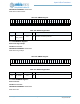
3
1
3
0
2
9
2
8
2
7
2
6
2
5
2
4
2
3
2
2
2
1
2
0
1
9
1
8
1
7
1
6
1
5
1
4
1
3
1
2
1
1
1
0
0
9
0
8
0
7
0
6
0
5
0
4
0
3
0
2
0
1
0
0
RSVD
LPMMODE
LPM_RD_WAIT
RSVD
SEDELAY
RD_WAIT
Table 223: FLASHCFG Register Bits
Bit Name Reset RW Description
31:14 RSVD 0x0 RO
This bitfield is reserved for future use.
Table 221: CACHECFG Register Bits
Bit Name Reset RW Description