
User Manual


Apollo3 Blue Datasheet
DS-A3-0p9p1 Page 160 of 909 2019 Ambiq Micro, Inc.
All rights reserved.
3.9.3.2.2 CACHECTRL Registers
3.9.3.2.2.1CACHECFG Register
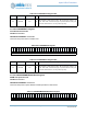
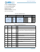
Flash Cache Control Register
OFFSET: 0x00000000
INSTANCE 0 ADDRESS: 0x40018000
Flash Cache Control Register
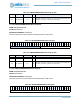
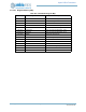
Table 220: CACHECFG Register
3
1
3
0
2
9
2
8
2
7
2
6
2
5
2
4
2
3
2
2
2
1
2
0
1
9
1
8
1
7
1
6
1
5
1
4
1
3
1
2
1
1
1
0
0
9
0
8
0
7
0
6
0
5
0
4
0
3
0
2
0
1
0
0
RSVD
ENABLE_MONITOR
RSVD
DATA_CLKGATE
RSVD
CACHE_LS
CACHE_CLKGATE
DCACHE_ENABLE
ICACHE_ENABLE
CONFIG
ENABLE_NC1
ENABLE_NC0
LRU
ENABLE
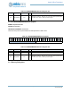
Table 221: CACHECFG Register Bits
Bit Name Reset RW Description
31:25 RSVD 0x0 RO
This bitfield is reserved for future use.
24
ENABLE_MONI-
TOR
0x0 RW
Enable Cache Monitoring Stats. Cache monitoring consumes additional
power and should only be enabled when profiling code and counters will
increment when this bit is set. Counter values will be retained when this is
set to 0, allowing software to enable/disable counting for multiple code seg-
ments.
23:21 RSVD 0x0 RO
This bitfield is reserved for future use.
20
DATA_CLK-
GATE
0x1 RW
Enable aggressive clock gating of entire data array. This bit should be set to
1 for optimal power efficiency.
19:12 RSVD 0x0 RO
This bitfield is reserved for future use.
11 CACHE_LS 0x1 RW
Enable LS (light sleep) of cache RAMs. Software should DISABLE this bit
since cache activity is too high to benefit from LS usage.
10
CACHE_CLK-
GATE
0x1 RW
Enable clock gating of cache TAG RAM. Software should enable this bit for
optimal power efficiency.
9
DCACHE_EN-
ABLE
0x0 RW
Enable Flash Data Caching.
8
ICACHE_EN-
ABLE
0x0 RW
Enable Flash Instruction Caching