
User Manual

Apollo3 Blue Datasheet
DS-A3-0p9p1 Page 147 of 909 2019 Ambiq Micro, Inc.
All rights reserved.
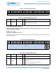
3.8.2.33 SRAMMODE Register
SRAM Controller mode bits
OFFSET: 0x00000284
INSTANCE 0 ADDRESS: 0x40020284
SRAM Controller mode bits
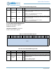
3.8.2.34 KEXTCLKSEL Register
Key Register to enable the use of external clock selects via the EXTCLKSEL reg
OFFSET: 0x00000348
INSTANCE 0 ADDRESS: 0x40020348
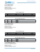
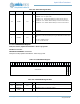
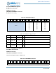
Table 195: SRAMMODE Register
3
1
3
0
2
9
2
8
2
7
2
6
2
5
2
4
2
3
2
2
2
1
2
0
1
9
1
8
1
7
1
6
1
5
1
4
1
3
1
2
1
1
1
0
0
9
0
8
0
7
0
6
0
5
0
4
0
3
0
2
0
1
0
0
RSVD
RSVD
DPREFETCH_CACHE
DPREFETCH
RSVD
IPREFETCH_CACHE
IPREFETCH
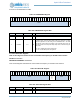
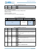
Table 196: SRAMMODE Register Bits
Bit Name Reset RW Description
31:8 RSVD 0x0 RO
RESERVED.
7:6 RSVD 0x0 RO
RESERVED.
5
DPREFETCH_-
CACHE
0x0 RW
Secondary prefetch feature that will cache prefetched data across bus wait-
states (requires DPREFETCH to be set).
4 DPREFETCH 0x0 RW
When set, data bus accesses to the SRAM banks will be prefetched (nor-
mally 2 cycle read access). Use of this mode bit is only recommended if the
work flow has a large number of sequential accesses.
3:2 RSVD 0x0 RO
RESERVED.
1
IPREFETCH_-
CACHE
0x0 RW
Secondary prefetch feature that will cache prefetched data across bus wait-
states (requires IPREFETCH to be set).
0 IPREFETCH 0x0 RW
When set, instruction accesses to the SRAM banks will be prefetched (nor-
mally 2 cycle read access). Generally, this mode bit should be set for
improved performance when executing instructions from SRAM.