
Data Sheet
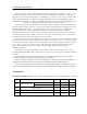
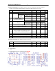

The Data Sheet of CH340 (the first) 7
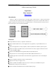
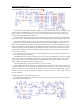
7.1.2 USB to RS232 Converter Configuration using CH340B
The image above use CH340T/CH340B (or CH340C
) to realize USB to RS232 converter. CH340 provides
common UART and MODEM signal, converts TTL to RS232 through level conversion chip U8. Port P11 is
DB9
connector, the pin and its function are the same as common PC DB9 connector, the chips similar with
U8 have MAX213/ADM213/SP213/MAX211
etc.
U8 and C46/C47/C48/C49/C40 could be removed when realize USB to TTL converter only. The signal lines in
the image only RXD、TXD and public ground need connected, the other signal lines should suspend when not use.
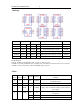
P2 is USB port, USB bus contains a pair of 5V power lines and a pair of data signal lines . Usually, the color of
+
5V power line is red, the black one is ground. D+ signal line is green and the D- signal line is white. The max
supply current of USB bus is up to 500mA. Generally, CH340 and low power consumption USB products can use
the 5V power supplied by USB bus directly. If the USB products supply standing power by other manner, CH340
should use this power too. If the USB bus power and standing power are necessary at the same time, connect a 1Ω
resistor between USB bus 5V power line and USB products 5V standing power line, and connect the ground lines
of these two power directly.
The capacitor C8
on V3 pin is 0.1uF, used to CH340 internal power node decoupling. The capacitor C9 is
0.1uF, used to external power decoupling.
For CH340G/T/R chip, Crystal X2, capacitor C6 and C7 are used for clock oscillation circuit. The X2 is 12MHz
quartz crystal, C6 and C7 are monolithic or high frequency ceramic capacitors with 22pF. If X2 is ceramic with low
cost, C6 and C7 must use the recommended value of crystal manufacturer and generally is 47pF. For the crystal
which is difficult to oscillate, halved value is suggested for C6.
Fo
r CH340C/E/B chip, crystal X2
and capacitor C6, C7 are not required.
When d
esigning the PCB, pay attention to: decoupling capacitor C8 and C9 must keep near to connection pin
of CH340; makes sure D+ and D- signal lines are parallel and supply ground lines or pour copper beside them to
decrease the interference from outside signal; the signal lines relevant to XI and XO should be kept as short as
possible. In order to lessen the high frequency interference, around the ground wire or pour copper around the
relevant components.
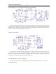
7.2. USB
to RS232 Converter Configuration (3-wire)
The
image below is USB to 3-wire RS232 converter design which is the most basic and most commonly used,
U5 uses MAX232/ICL232/SP232 etc.