Version: B Issued Date: 2018/06/12 Approval Sheet (產品承認書) 產品名稱 (Product): BT 5.0 Module (nRF52840) 產品型號 (Model No.): MDBT50Q – 1M (Chip Antenna) MDBT50Q – P1M (PCB Antenna) Working distance of MDBT50Q-1M & MDBT50Q-P1M: ⚫ 1Mbps: MDBT50Q: over 300 meters in open space. MDBT50Q-P: up to 250 meters in open space. ⚫ 2Mbps: MDBT50Q: over 150 meters in open space. MDBT50Q-P: up to 120 meters in open space.
Index 1. Overall Introduction ...................................................................................................... 3 1.1. Application ............................................................................................................ 3 1.2. Features ............................................................................................................... 4 2. Product Dimension .................................................................................................
1. Overall Introduction Raytac’s MDBT50Q & MDBT50Q-P is a BT 5.0 stack (Bluetooth low energy or BLE) module designed based on Nordic nRF52840 SoC solution, which incorporates: GPIO, SPI, UART, I2C, I2S, PMD, PWM, ADC, NFC and USB interfaces for connecting peripherals and sensors. Features of the module: 1. Embedded 2.4GHz transceiver supports Bluetooth 5, IEEE 802.15.4 & 2.4Ghz RF & ANT upon customer’s preference. 2. Compact size with (L) 15.5 x (W) 10.5 x (H) 2.2 or 2.0 mm. 3.
1.2. Features ‧Bluetooth 5, IEEE 802.15.4, 2.4 GHz transceiver ‧-95dBm sensitivity in 1Mbps Bluetooth low energy (BLE) mode ‧-103dBm sensitivity in 125Kbps BLE mode (long range) ‧+8 dBm TX power (down to -20 dBm in 4 dB steps) ‧On-air compatible with nRF52, nRF51, nRF24L and nRF24AP Series ‧Programmable output power from +8dBm to -20dB ‧RSSI (1dB resolution) ‧Supported data rates: ‧Bluetooth 5: 2 Mbps, 1 Mbps, 500 kbps, 125 kbps ‧IEEE 802.15.4-2006: 250 kbps ‧Proprietary 2.
‧Flexible power management ‧Supply voltage range 1.7V to 5.5V ‧On-chip DC/DC and LDO regulators with automated low current modes ‧Regulated supply for external components from 1.8V to 3.3V ‧Automated peripheral power management ‧Fast wake-up using 64MHz internal oscillator ‧0.4uA at 3V in OFF mode, no RAM retention ‧1.
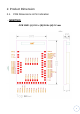
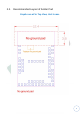
2. Product Dimension 2.1. PCB Dimensions & Pin Indication ‧MDBT50Q PCB SIZE: (L) 15.5 x (W) 10.5x (H) 2.
‧MDBT50Q-P PCB SIZE: (L) 15.5 x (W) 10.5 x (H) 2.
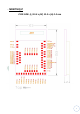
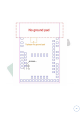
2.2. Recommended Layout of Solder Pad Graphs are all in Top View, Unit in mm.
2.3. RF Layout Suggestion (aka Keep-Out Area) Please follow below instruction to have better wireless performance. Make sure to keep the “No-Ground-Pad” as wider as you can when there is no enough space in your design. Welcome to send us your layout in PDF for review at service@raytac.com with title “Layout reviewing – MDBT50Q/MDBT50Q-P – YOUR company’s name”.
Examples of “NOT RECOMMENDED” layout 14
2.4. Pin Assignment Pin No. Name Pin Function Description (1) GND Power Ground (2) GND Power Ground (3) P1.10 Digital I/O (4) P1.11 Digital I/O (5) P1.12 Digital I/O (6) P1.13 Digital I/O (7) P1.14 Digital I/O (8) P1.15 Digital I/O P0.03 Digital I/O AIN1 Analog input P0.29 Digital I/O AIN5 Analog input P0.02 Digital I/O AIN0 Analog input P0.31 Digital I/O AIN7 Analog input P0.
Pin No. Name Pin Function Description P0.30 Digital I/O AIN6 Analog input (15) GND Power (16) P0.27 Digital I/O General-purpose I/O P0.00 Digital I/O General-purpose I/O XL1 Analog input P0.01 Digital I/O XL2 Analog input P0.26 Digital I/O General-purpose I/O P0.04 Digital I/O General-purpose I/O AIN2 Analog input P0.05 Digital I/O AIN3 Analog input P0.06 Digital I/O General-purpose I/O P0.07 Digital I/O General-purpose I/O TRACECLK Trace clock (24) P0.
Pin No. Name Pin Function (33) GND Power Ground (34) D˗̶̶̶ Digital I/O USB D- (35) D+ Digital I/O USB D+ (36) P0.14 Digital I/O General-purpose digital I/O (37) P0.13 Digital I/O General-purpose digital I/O (38) P0.16 Digital I/O General-purpose digital I/O (39) P0.15 Digital I/O General-purpose digital I/O P0.18 Digital I/O (40) nRESET Description General-purpose digital I/O (recommended usage: QSPI / CSN) Configurable as system RESET (41) P0.17 Digital I/O (42) P0.
Pin No. Name Pin function P0.10 Digital I/O NFC2 NFC input (55) GND Power (56) P1.04 Digital I/O (57) P1.06 Digital I/O (58) P1.07 Digital I/O (59) P1.05 Digital I/O (60) P1.03 Digital I/O (61) P1.01 Digital I/O Description General-purpose I/O (standard drive, low frequency I/O only) (54) 2.5.
4. Shipment Packaging Information Antenna Model MDBT50Q-1M Chip/Ceramic Antenna MDBT50Q-P1M PCB/Printed Antenna - Unit Weight of Module: MDBT50Q-1M: 0.68g / pc (±0.02g) ; MDBT50Q-P1M: 0.64g / pc (±0.02g) - Packaging Type: Tray only - Minimum Package Quantity (MPQ): 88 pcs per Tray - Carton Contents: 1760 pcs per carton (20 Full Tray + 1 Empty Tray) - Dimension of Carton: (L) 37 x (W) 21 x (H) 13 cm - Gross Weight: approx. 2.
5. Specification Any technical spec shall refer to Nordic’s official documents as final reference. 5.1. Absolute Maximum Ratings 5.2.
5.3. Electrical Specifications 5.3.1. General Radio Characteristics 5.3.2.
5.3.3. Radio Current Consumption (Receiver) 5.3.4.
5.3.5. Receiver Operation 5.3.6.
5.3.7.
5.3.8. Radio Timing Parameters 5.3.9. RSSI Specifications 5.3.10.
5.3.11.
6.
7. Antenna 7.1.
7.2.
8. Reference Circuit Module’s default is using “DC-DC mode”, and must connect it to external 32.768khz to work. REMARK: ** When NOT using DC-DC (VDDH) mode, please remove L4. ** (L4 spec: 10𝛍H, 0603 Chip Inductor, IDC, min = 80mA, ±𝟐𝟎%) ** When NOT using NFC, please remove NFC1 / C19 / C21. ** ** When using internal 32.768khz RC oscillator, please remove X2 / C12 / C13.
9. Certification All certifications are pending. It is estimated to be available in July of 2018. 10. Notes and Cautions Module is not designed to be used and lasting a lifetime. Like general products, it is expected to be worn out after continuous usage through the years. To assure that product will perform better and last longer, please ⚫ Follow the guidelines of this document while designing circuit/end-product.
11. Basic Facts for nRF52 Chip Below is the comparison chart between nRF52840, nRF52832 and nRF52810. Any discrepancy shall refer to Nordic’s technical document as final reference. nRF52840 RAYTAC Model No.: Bluetooth 5 Long Range (x4) nRF52832 nRF52810 Click to see “Full List of Raytac’s BLE Modules” V Bluetooth 5 V V V V V V Flash (kBytes) 1024 512 192 RAM (kBytes) 256 64 24 ANT V V V IEEE 802.15.
12. Useful Links ⚫ Nordic Infocenter: https://infocenter.nordicsemi.com/index.jsp All the necessary technical files and software development kits of Nordic’s chip are on this website. ⚫ Nordic Developer Zone: https://devzone.nordicsemi.com/questions/ A highly recommended website for firmware developer. Interact with other developers and Nordic’s employees will help with your questions. The site also includes tutorials in detail to help you get started. ⚫ Official Page of nRF52840 : https://www.
Full List of Raytac’s BLE Modules MDBT40 & MDBT40-P Series Series Nordic Solution MDBT40 nRF51822 MDBT40-P nRF51822 MDBT40 - ANT nRF51422 IC Version Antenna RAM Flash Memory 3 Chip Antenna 16 kb 256 K 32 kb 256 K 3 PCB Antenna 16 kb 256 K 32 kb 256 K MDBT40-ANT -256V3 MDBT40-ANT -256RV3 3 Chip Antenna MDBT40-ANT -P256V3 MDBT40-ANT -P256RV3 3 Raytac No.
MDBT42Q Series (QFN Package IC) Series Nordic Solution Raytac No.
Release Note ⚫ 2017/10/30 Pre-release ⚫ 2018/01/19 Model no. officially changed to MDBT50Q-1M & MDBT50Q-P1M. ⚫ 2018/04/10 Version A (1st release) ⚫ 2018/06/12 Version B (1) Added Chapter 4: Shipment Packaging Info and Chapter 7: Antenna.