
Data Sheet

The DataSheet of CH340 (the first) 4
one high-level stop bit. Supporting odd check/even check/flag check/blank check. CH340 supports common
baud rate: 50,75,100,110,134.5,150,300,600,900,1200,1800,2400,3600,4800,9600,14400,19200,28800,
33600,38400, 56000,57600,76800,115200,128000,153600,230400,460800,921600,1500000,2000000 and so
on. The baud rate error of serial transfer signal is less than 0.3%, and permission baud rate error of serial
receive signal is not less than 0.2%.
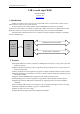
In the WINDOWS operation system of computer endpoint, drive program of CH340 can communicate
standard serial interface. So the mostly original serial interface application program is totally compatible,
and without any modify.
CH340 can be used to upgrade the former serial interface peripheral equipment, or add extra serial
interface for computer via USB bus. Supply RS232, RS485, RS422 and other interface via adding level
change device.
Only add infrared transceiver, CH340 can add SIR infrared adapter for computer via USB bus, realize
infrared communication between computer and peripheral equipment which is according to IrDA criterion.
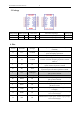
6. Parameter
6.1. Absolute maximum rating (Stresses above those listed can cause permanent damage to the device.
Exposure to maximum rated conditions can affect device operation and reliability.)
Name
Parameter note Min. Max. Units
TA Ambient operating temperature -40 85 ℃
TS Storage temperature -55 125 ℃
VCC
Voltage source (VCC connects to power, GND to ground)
-0.5 6.5 V
VIO
The voltage of input or output pin -0.5 VCC+0.5 V
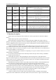
6.2. Electrical parameter (test conditions: TA=25℃, VCC=5V, exclude pin connection of USB bus)
(The every current parameter must multiply the coefficient of 40% when the power is 3.3V)
Name
Parameter note Min. Typical
Max. Units
V3 doesn’t connect to VCC 4.5 5 5.3
VCC Source voltage
V3 connect to VCC 3.3 3.3 3.8
V
ICC Total source current when working 12 30 mA
VCC=5V 0.15 0.2 mA
ISLP
Total source current when
USB suspending
VCC=3.3V 0.05 0.08 mA
VIL Input Voltage LOW -0.5 0.7 V
VIH Input Voltage HIGH 2.0 VCC+0.5
V
VOL Output Voltage LOW (draw 4mA current) 0.5 V
VOH
Output Voltage HIGH (output 3mA current)
(Output 100uA current during chip reset)
VCC-0.5
V
IUP Input current with pull-up resistor internal 3 150 300 uA
IDN Input current with pull-down resistor internal -50 -150 -300 uA
VR Restrict voltage when power-up reset 2.3 2.6 2.9 V
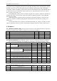
6.3. sequence parameter (test conditions: TA=25℃,VCC=5V)
Name Parameter note Min. Typical
Max. Units
FCLK Frequency of input clock in XI 11.98 12.00 12.02 MHz
TPR Reset time of power-up 20 50 mS